
 Login
Login Register
 Submit a Paper
 Propose a Special lssue
 Open Access
ARTICLE

Investigation of Sputtered TiO2 Thin Films and Modeling of TiO2-Based Heterojunctions with p-Si and p-GaAs
1 Energy and Materials Engineering Laboratory (LGEM), Faculty of Science and Technology, Sultan Moulay Slimane University, Beni-Mellal, Morocco
2 Material Sciences Unit (USM), DERS, National Center for Energy, Sciences and Nuclear Techniques (CNESTEN), Rabat, Morocco
3 Research Center on Advanced Materials and Technologies (RAMTECH), Department of Exact and Natural Sciences, Institute of Interdisciplinary Research, Alexandru Ioan Cuza University of Iasi, 11 bd. Carol I, Iasi, Romania
4 Laboratory of Industrial Engineering and Surface Engineering, Faculty of Science and Technology, University Sultan Moulay Slimane, Beni Mellal, Morocco
* Corresponding Authors: Sana Handor. Email: ; Abdelati Razouk. Email:
(This article belongs to the Special Issue: Advances and Emerging Trends in Photovoltaic Technologies, Energy Storage, and Green Hydrogen)
Energy Engineering 2026, 123(9), 11 https://doi.org/10.32604/ee.2026.082739
Received 21 March 2026; Accepted 07 May 2026; Issue published 06 August 2026
 View Full Text
 Download PDF
Abstract
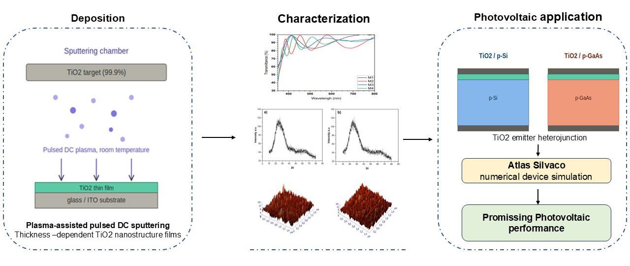
In this study, thin films of titanium dioxide (TiO2) were deposited onto glass and indium tin oxide (ITO) substrates at room temperature, using plasma-assisted pulsed DC sputtering with a 99.9% pure stoichiometric TiO2 target. Our research aims to investigate the influence of film thickness on the optical, structural, and morphological properties of TiO2 nanostructured thin films, as well as its impact on the photovoltaic performance of heterojunctions where TiO2 serves as the emitter. Using advanced PRISA software, parameters such as refractive index, film thickness, and band gap energy were determined. Spectrophotometry analysis shows that TiO2 thin film samples exhibited up to 90% optical transparency in the UV-Vis spectral region. Using X-ray diffraction (XRD) analysis revealed an amorphous phase, particularly at lower scan angles, while atomic force microscopy (AFM) images show an homogeneous surface of deposited films with low roughness. A notable reduction in the optical band gap was observed with increasing film thickness. Finally, numerical simulations of TiO2/p-Si and TiO2/p-GaAs heterojunction Solar cells, performed using Atlas SILVACO software, predict promising photovoltaic performance based on the optical data of the elaborated TiO2 thin films.Graphic Abstract
Keywords
Thin films have become essential component in various technological applications, ranging from microelectronics to optoelectronics and energy harvesting devices [1,2]. Among the diverse fabrication methods, such as spin coating [3] and spray coating [4], magnetron sputtering [5] is one of the most commonly used techniques for producing thin films, it is a physical vapor deposition method that allows precise control over film thickness and composition.
DC magnetron sputtering is a widely used method for depositing thin TiO2 films in a precise and controlled way. By combining magnetron sputtering with reactive gas chemistry, this technique makes it possible to manage the composition and stoichiometry of the resulting thin film. One of its key advantages is that it produces high-quality, uniform coatings that bond strongly to the substrate, which in turn enhances the durability and long-term stability of the deposited film. What makes this technique especially practical is that the film’s final properties can be tuned simply by adjusting a few process parameters, including the argon/oxygen flow rate, sputtering power, chamber pressure, and target composition. In a typical DC magnetron sputtering setup, argon gas is introduced into the chamber to generate a plasma, which produces the ions needed to bombard the target material. Oxygen is then added alongside argon to react with the deposited atoms and help control the chemical makeup of the growing film [6–8].
In the case of TiO2 films, the relationship between argon and oxygen is particularly important. Argon drives the sputtering process by generating the ions and controlling the flux of particles reaching the substrate, while oxygen determines the film’s stoichiometry by governing the surface chemical reactions and influencing the mobility of deposited species. Together, these two gases work in tandem to shape the final structure and performance of the TiO2 film [9].
TiO2 has advantageous optical properties and excellent chemical stability, and it is among the most widely used high-refractive-index materials and films, and also offers good mechanical stability and hardness [10]. Their ability to grow on unheated substrates has long attracted the attention of researchers, as it paves the way for the large-scale production of inexpensive and adaptable coatings. The given crystalline structure of TiO2 can influence its properties, with anatase being more active than rutile in terms of photocatalytic activity [11]. However, even amorphous TiO2 nanoparticles have demonstrated beneficial photocatalytic properties, particularly for the fabrication of microstructures [12].
Among semiconductor materials used in photocatalysis and photovoltaics, TiO2 stands out as a stable and non-toxic compound. In dye-sensitized solar cells, TiO2 serves as a key material that enables efficient dye loading charge transport [13]. In perovskite solar cells, TiO2 is widely used as an electron transport layer (ETL), where its wide bandgap, suitable energy alignment, and high electron mobility reduce recombination losses and enhance overall device efficiency. Ongoing research on TiO2 thin films is driven by the need to optimize their structural, morphological, and electronic properties to further improve charge extraction, light harvesting, and overall device performance in cost-effective solar energy systems [14,15].
This study explores the effect of film thickness on the optical properties of TiO2 thin films deposited by plasma-assisted magnetron sputtering. It uses the envelope method, implemented in the PRISA software via a Python module [16], to determine the film thickness and optical constants from transmittance curves obtained by spectrophotometry. The optical data are then used for numerical simulations of two heterojunction solar cells—TiO2/p-Si and TiO2/p-GaAs using SILVACO Atlas software [17]. These simulations aim to explore and optimize the electronic and photovoltaic performance of the heterojunctions, in which TiO2 serves as an electron transport layer (ETL) to improve charge separation and transport.
The scientific novelty of this work lies in the integrated experimental–numerical approach, which provides a quantitative link between plasma-assisted sputtering parameters, structural film evolution, and the resulting photovoltaic performance of TiO2-based heterojunctions. By explicitly correlating thickness-dependent optical constants with device-level carrier dynamics, this research offers a refined framework for optimizing TiO2 electron transport layers in cost-effective photovoltaic architectures.
Developing methods to determine crucial components of thin films, such as absorption coefficient and the dispersion of the refractive index has garnered significant interest. Only a select few of these techniques have been established, including ellipsometry, fitting methods [18], and reflection spectrum method [19].
In systems where an absorbing thin film is deposited on a transparent substrate, light enters the substrate, interacts with the deposited film, and exits the substrate after multiple internal reflections. This scenario is commonly observed in waveguide-like systems, where the transparent substrate confines light within the structure. A schematic representation of such a system, where d is the film thickness and N is a complex refractive index N = n − ik, is shown in Fig. 1. Here, n is the refractive index, and k denotes the extinction coefficient [20].

Figure 1: Characterizing an absorbent thin film on a substantial, finite transparent substrate.
The transmission T in Fig. 1 is a complex function given by:
s being known, it is convenient to write the above equation in terms of n(λ) and the absorbance x (λ), where x is defined in equation T = T (n, x); expressed as:
where;
A = 16 n2s
B = (n − 1)3(n + s2)
C = 2(n2 − 1) (n2 − s2)
D = (n − 1)3 (n − s2)
Φ = 4πnd/λ
x = exp(−αd)
where:
s is the substrate refractive index.
When considering films for adjacent wavelengths λ1 and λ2, n1 and n2 represent the refractive indices of the nanostructures, respectively. We obtain the thickness of nanostructures by referring to the following equation:
TiO2 films were deposited at room temperature onto glass and Indium Tin Oxide (ITO) substrates using plasma-assisted pulsed DC sputtering. A ceramic stoichiometric TiO2 target with 99.9% purity, and 7.62 cm in diameter, served as the cathode in the magnetron discharge. The deposition process was done in a chamber with a base pressure of 2.0 × 10⁻⁵ mbar. A high-purity Ar–O2 gas mixture was used, with the gas pressure maintained at 1.3 × 10⁻² mbar by automatic flowmeter regulators.
The substrates were positioned 6 cm from the cathode target, the pulsed DC discharge was operated at 100 W (t = 5 μs, υ = 5 kHz). The deposition durations were set to 2 and 3 h 20 min, producing Titanium Dioxide films with thickness ranging from 200 to 500 nm, respectively. The details of all prepared samples are summarized in Table 1.

As shown in Fig. 2, interference bands are observed in the transmittance spectra at wavelengths extending beyond the visible spectrum. This phenomenon arises from the multiple reflections of radiation between the lower surface (in contact with either glass or an ITO substrate) and the free surface of the Titan dioxide layer [21]. These interference bands in the transmittance spectra show that the TiO2 films produced are of consistent and uniform thickness. Furthermore, this suggests that the surfaces are smooth and exhibit homogeneity. With increasing thickness, we noticed a corresponding increase in the number of interference bands and they become closer together. At low thicknesses, incomplete absorption occurs between 350 and 400 nm, producing a noticeable shoulder in the spectrum. This shoulder appears at higher thicknesses, where the film can absorb all the incident light.

Figure 2: Transmittance T spectra of TiO2 nanofilms deposited at different thicknesses on glass and ITO.
PRISA software was used to calculate optical constants, dispersion parameters, absorption coefficient, bandgap energy and thickness from the spectrophotometric transmission data. In order to apply this method, the absorption coefficient for the TiO2 films was calculated based on the transmittance spectra (as illustrated in Fig. 3) as it is previously mentioned. No significant difference in bandgap energy is observed between samples of the same thickness deposited on glass vs. ITO. However, a small variation is observed when comparing samples of different thickness, which allows to concluded that TiO2 thin films showed a decrease in optical band gap from 3.65 to 3.41 eV and from 3.59 to 3.47 eV for glass and ITO respectively, with increasing thickness of the deposited films. It should be noted that all bandgap values (Table 2) are in line with what was expected according to the literature.

Figure 3: TMax and Tmin transmittance curves for TiO2 sputtered sample on glass.

However, the bandgap values depend on the crystallinity and thickness of the coatings, leading to the conclusion that control of these factors is fundamental to the creation of films with photocatalytic properties. Furthermore, Fig. 2 shows a spectrum resulting from interference effects at constant thickness d. These patterns of light and dark bands, rather than being annoying, serve to determine the optical properties of the film, as shown in Table 2 and studied in this research.
Fig. 4 shows the X-ray diffraction (XRD) patterns of TiO2 thin films deposited on ITO substrates of two different thicknesses (415 and 508 nm). Despite the use of a 3° incidence angle, the diffraction patterns exhibit a background largely devoid of features, indicating an amorphous or weakly crystalline structure. The broad signal at small angles is mainly attributed to the amorphous nature of the glass substrate, which is consistent with literature [22,23]. In thin films deposited on disordered or conductive substrates, such as ITO/glass, XRD signals are often attenuated due to limited substrate interference and long-range order, making peak resolution difficult.

Figure 4: Diffractograms of TiO2 thin films deposited on glass with different Thickness/(a)—XRD sputtered sample M1, (b)—XRD sputtered sample M2.
The amorphous nature of the sputtered TiO2 films, characterized by a lack of long-range crystalline order, has profound implications for photovoltaic performance. Amorphous transition metal oxides inherently possess a high density of localized sub-bandgap states, primarily associated with oxygen vacancies and uncoordinated Ti ions. These deep-level defects act as potent Shockley-Read-Hall (SRH) non-radiative recombination centers. Consequently, this structural disorder severely impedes bulk electron mobility and restricts the minority carrier diffusion length, ultimately manifesting as a reduction in the open-circuit voltage (VOC) and fill factor (FF). However, while the amorphous phase introduces these localized defect states, it simultaneously facilitates a superior surface morphology. This ultra-smooth, continuous interface (as confirmed by AFM) is highly advantageous for achieving conformal contact and mitigating parasitic shunt pathways, representing a critical engineering trade-off for optimizing the electronic homogeneity of the heterojunction interface.
Fig. 5a,b shows AFM images of TiO2 thin films, which reveal the morphology and surface roughness of the deposited layers. The micrographs show homogeneous, continuous films with low roughness values of 1.7 and 1.5 nm, respectively, for samples with thicknesses of 415 and 508 nm. This smooth morphology is favorable for the deposition of further layers in solar cell architectures, as it provides a good interface contact and reduces shunt pathways.

Figure 5: (a)—AFM of TiO2 sample sputtered M1. (b)—AFM of TiO2 sample sputtered M2. (c) Line profile of TiO2 layer M1. (d) Line profile of TiO2 layer M2.
Furthermore, the line profiles shown in Fig. 5c,d indicates the presence of interconnected nanoscale cavities in the TiO2 films. This porous morphology increases the effective surface area, which can facilitate the infiltration of active materials during device fabrication. Such structural characteristics are particularly beneficial in photovoltaic devices, where improved interfacial contacting can facilitate charge transport despite the limited crystallinity of the TiO2 layer.
4.3 Simulation of TiO2/p-Si and TiO2/p-GaAs Heterojunction Solar Cells
The Silvaco ATLAS device simulator was used in this section to examinate, how the thickness of experimentally obtained TiO2 thin films by DC magneton sputtering, can influence the performance of photovoltaic devices when combined with Si and GaAs absorbers.
ATLAS Silvaco is a physically-based simulator of semiconductor devices, which predicts the electrical and photoelectric behavior and provides insights on internal physical processes involved in the device functionality. The numerical simulation is based on the resolution of Poisson equation (Eq. (6)) and electron and hole continuity equations (Eqs. (7) and (8)) [24]:
where ε is the local permittivity, Ψ is the electrostatic potential, q is the elementary charge and
where
The photogeneration rate is modeled in ATLAS Silvaco by the following Equation:
where P is the ray intensity factor, which contains the cumulative effects of reflections, transmissions, and loss due to absorption over the ray path;
where k is the extinction coefficient.
The numerical simulations employed Fermi-Dirac statistics model to described the carrier behavior, while the drift-diffusion model was used for carrier transport. Recombination mechanisms, including Shockley-Read-Hall, Auger, and radiative recombination (nonradiative recombination model is applied for Si material), were incorporated to account for carrier losses in the interfaces and in the bulk. These combined models ensure that the simulation reflects the essential physical phenomena of the structures under study. Neumann boundary conditions (zero flux conditions) and Dirichlet conditions (ohmic boundary conditions) were applied along the lateral edges and at the electrodes, respectively. All material properties including mobility, electron affinity, and recombination parameters were taken from widely accepted values in the literature to ensure consistency with previously documented experimental devices. The physical parameters of TiO2, Si, and GaAs are illustrated in Table 3.

The solar cells were irradiated under standard AM1.5G conditions with an intensity of 100 mW/cm2. The photovoltaic parameters, including short circuit current density (JSC), open-circuit voltage (VOC), fill factor (FF), and power conversion efficiency, were then extracted from simulated J-V characteristics and analyzed as a function of TiO2 Thickness for TiO2/p-Si and TiO2/p-GaAs heterojunction solar cells.
The simulated current density-voltage (J-V) curves for the two structures are shown in Figs. 6 and 7, and the resulting photovoltaic parameters are listed in Table 4. As can be observed, the highest conversion efficiencies achieved are 10.80% for TiO2/p-Si structures and 18.24% for TiO2/p-GaAs structures, indicating that the TiO2/p-GaAs structure has a higher overall efficiency than the silicon-based device. This improvement is due to the intrinsic properties of GaAs, which possesses a high optical absorption coefficient, approximately 104 times greater than that of silicon [28], and a direct bandgap that minimizing non-radiative recombination, Enabling more efficient charge extraction. Furthermore, GaAs offers higher carrier mobility, which reduces transport losses and helps improve device performance. This results in a higher open-circuit voltage (Voc ≈ 0.944 V), which is consistent with the wider bandgap of GaAs (1.42 eV).

Figure 6: I–V curves of simulated TiO2/p-Si heterojunction with different TiO2 layer properties.

Figure 7: I–V curves of simulated TiO2/p-GaAs heterojunction with different TiO2 layer properties.

In contrast, the TiO2/p-Si structure exhibits a relatively higher short-circuit current density (JSC). This behavior can be explained by the longer carrier lifetime in crystalline silicon, which reduces losses due to bulk recombination and allows a higher number of photogenerated carriers to contribute to the current. It is also important to note that, while GaAs-based devices offer higher conversion efficiency, this comes with more expensive materials and more complex manufacturing requirements. In contrast, silicon-based devices, despite their lower efficiency, remain more attractive for large-scale, low-cost photovoltaic applications.
The optical properties of TiO2, such as the refractive index (n), extinction coefficient (k), and absorption coefficient, have a significant impact on the amount of light reaching the absorber layer. More particularly, the variation in film thickness changes the optical response of the TiO2 emitter by modifying the structural quality and surface morphology [29,30], which in turn affect light transmitted the emitter and, consequently, the electron-hole generation rate at the absorber. Furthermore, the TiO2 thickness variation affects the resistivity of the emitter region, thereby impacting the series resistance and consequently the fill factor of the device [31,32]. These combined effects explain the observed variations in photovoltaic parameters as a function of TiO2 thickness, where improvements are mainly observed in the fill factor, while the short-circuit current density and open-circuit voltage remain largely unchanged.
In this study, the selected deposition parameters enabled the fabrication of thin and transparent TiO2 films with high optical transmittance. In particular, films deposited for 2 h showed few interference fringes, also the bandgap of thin TiO2 films was found to vary depending on their thickness and crystalline structure. By comprehending and manipulating these variables in the plasma deposition technique, we can create films tailored for specific uses. These transparent and conductive films exhibit desirable photocatalytic properties, as it is highlighted in the simulation part TiO2 thin films show promise as functional components of photovoltaic systems, particularly when combined with light-absorbing materials of the p-silicon (Si) and gallium arsenide (GaAs) types. Our simulation indicates that fine-tuning the thickness of the TiO2 layer improves the fill factor (FF), boosting overall efficiency without adversely affecting short-circuit current density (Jsc) or open-circuit voltage (Voc). The study demonstrates maximum conversion efficiencies of 10.80% for TiO2/p-Si and 18.24% for TiO2/p-GaAs heterojunctions, underlining the adaptability and efficiency of TiO2 thin films in solar energy applications.
The findings highlight a critical device engineering trade-off: while the direct bandgap and high electron mobility of GaAs yield superior overall efficiency and voltage (VOC), the intrinsically longer minority carrier lifetime of crystalline silicon ensures a highly robust short-circuit current (JSC) in a much more economically scalable architecture.
These findings pave the way for future innovations in photovoltaic technology, emphasizing the critical role of precise material engineering in achieving high-performance solar energy devices.
Acknowledgement: The authors gratefully acknowledge the financial support provided through the Erasmus+ mobility project (2020-1-RO01-KA107-078499). The authors also express their sincere appreciation to University Sultan Moulay Slimane and Alexandru Ioan Cuza University of Iasi for their valuable support and contributions.
Funding Statement: Research funded by Erasmus+ 2020-1-RO01-KA107-078499.
Author Contributions: Sana Handor carried out experimental work at RAMTECH and wrote the manuscript. Mohamed Manoua realized the simulation part and writing. Laura Hrostea, Liviu Leontie: directed experimental work and results interpretation. Abdelati Razouk, Mohamed Sahlaoui: supervision, validation of results and co-writing. Mohammed Sajieddine, Mustapha Adar: orientation and planning. All authors reviewed and approved the final version of the manuscript.
Availability of Data and Materials: The data that support the findings of this study are available from the Corresponding Author, Sana Handor, upon reasonable request.
Ethics Approval: Not applicable.
Conflicts of Interest: The authors declare no conflicts of interest.
References
1. Devasahayam S, Hussain CM. Thin-film nanocomposite devices for renewable energy current status and challenges. Sustain Mater Technol. 2020;26(2):e00233. doi:10.1016/j.susmat.2020.e00233. [Google Scholar] [CrossRef]
2. Wu YN, Wuenschell JK, Fryer R, Saidi WA, Ohodnicki P, Chorpening B, et al. Theoretical and experimental study of temperature effect on electronic and optical properties of TiO2: comparing rutile and anatase. J Phys Condens Matter. 2020;32(40):ab9d4f. doi:10.1088/1361-648X/ab9d4f. [Google Scholar] [PubMed] [CrossRef]
3. Tomulescu AG, Stancu V, Beşleagă C, Enculescu M, Nemneş GA, Florea M, et al. Reticulated mesoporous TiO2 scaffold, fabricated by spray coating, for large-area perovskite solar cells. Energy Tech. 2020;8(1):1900922. doi:10.1002/ente.201900922. [Google Scholar] [CrossRef]
4. Handor S, Tomulescu AG, Stancu V, Razouk A, Galca AC, Leonat LN. Gas-assisted spray fabrication of reticulated TiO2 scaffolds for perovskite solar applications. Micromachines. 2025;16(6):685. doi:10.3390/mi16060685. [Google Scholar] [PubMed] [CrossRef]
5. Zhang L, Liu H, Chen H, Chen Y, Li N, Tan C, et al. Preparation of amorphous TiO2 films by RF magnetron sputtering: process optimization and effect of sputtering pressure on electrochromic properties. Phys B Condens Matter. 2025;697:416726. doi:10.1016/j.physb.2024.416726. [Google Scholar] [CrossRef]
6. Sezgin A, Čtvrtlík R, Václavek L, Tomáštík J, Nožka L, Menşur E, et al. Optical, structural and mechanical properties of TiO2 and TiO2-ZrO2 thin films deposited on glass using magnetron sputtering. Mater Today Commun. 2023;35(2):106334. doi:10.1016/j.mtcomm.2023.106334. [Google Scholar] [CrossRef]
7. Dave DP, Chauhan KV. Synthesis of visible spectrum-active TiO2 thin film induced by RF magnetron sputtering. Mater Today Proc. 2022;62:4254–9. doi:10.1016/j.matpr.2022.04.755. [Google Scholar] [CrossRef]
8. Villamayor A, Pomone T, Perero S, Ferraris M, Barrio VL, G-Berasategui E, et al. Development of photocatalytic nanostructured TiO2 and NiO/TiO2 coatings by DC magnetron sputtering for photocatalytic applications. Ceram Int. 2023;49(11):19309–17. doi:10.1016/j.ceramint.2023.03.058. [Google Scholar] [CrossRef]
9. Eleutério T, Sério S, Vasconcelos HC. Growth of nanostructured TiO2 thin films onto lignocellulosic fibers through reactive DC magnetron sputtering: a XRD and SEM study. Coatings. 2023;13(5):922. doi:10.3390/coatings13050922. [Google Scholar] [CrossRef]
10. O’Byrne M, Kerzabi B, Abbarchi M, Lifschitz A, Zamora T, Malgras V, et al. Investigation of the anatase-to-rutile transition for TiO2 sol-gel coatings with refractive index up to 2.7. Thin Solid Films. 2024;790:140193. doi:10.1016/j.tsf.2023.140193. [Google Scholar] [CrossRef]
11. Barrocas B, Monteiro OC, Jorge ME, Sério S. Photocatalytic activity and reusability study of nanocrystalline TiO2 films prepared by sputtering technique. Appl Surf Sci. 2013;264:111–6. doi:10.1016/j.apsusc.2012.09.136. [Google Scholar] [CrossRef]
12. Song C, Xiao L, Chen Y, Yang F, Meng H, Zhang W, et al. TiO2-based catalysts with various structures for photocatalytic application: a review. Catalysts. 2024;14(6):366. doi:10.3390/catal14060366. [Google Scholar] [CrossRef]
13. Hnawi SK, El Mansouri A, Abdallah N, Agdad A, Tchenka A, Cheikh S, et al. Investigation of Aloe Vera latex used as natural dye in TiO2-based heterojunction and liquid-electrolyte dye-sensitized solar cells. J Sol Energy Eng. 2022;144(5):051002. doi:10.1115/1.4054029. [Google Scholar] [CrossRef]
14. Zhu H, Zhang TH, Wei QY, Yu SJ, Gao H, Guo PC, et al. Preparation of TiO2 electron transport layer by magnetron sputtering and its effect on the properties of perovskite solar cells. Energy Rep. 2022;8:3166–75. doi:10.1016/j.egyr.2022.02.068. [Google Scholar] [CrossRef]
15. Derbali S, Nouneh K, Leonat LN, Stancu V, Tomulescu AG, Galca AC, et al. Partial replacement of Pb2+ in MAPbI2·6Cl0.4 perovskite films and their photovoltaic performance. J Mater Sci Mater Electron. 2023;34(10):903. doi:10.1007/s10854-023-10318-9. [Google Scholar] [CrossRef]
16. Jena S, Tokas RB, Thakur S, Udupa DV. PRISA: a user-friendly software for determining refractive index, extinction co-efficient, dispersion energy, band gap, and thickness of semiconductor and dielectric thin films. Nano Express. 2021;2(1):010008. doi:10.1088/2632-959X/abd967. [Google Scholar] [CrossRef]
17. Manoua M, Jannane T, Abouelala O, Fazouan N, Almaggoussi A, Kamoun N, et al. Modeling and optimization of n-ZnO/p-Si heterojunction using 2-dimensional numerical simulation. Eur Phys J Appl Phys. 2020;90(1):10101. doi:10.1051/epjap/2020190333. [Google Scholar] [CrossRef]
18. Blond J, Dufour C, Chaluvadi SK, Duprey S, Portier X, Marie P, et al. Optical constants and thickness determination of La2/3 Sr1/3 MnO3 thin films on Nb: SrTiO3 substrates by spectro-ellipsometry: combination of optical and X-ray techniques. Appl Surf Sci. 2024;669(11):160489. doi:10.1016/j.apsusc.2024.160489. [Google Scholar] [CrossRef]
19. Wang YH, Rahman KH, Wu CC, Chen KC. A review on the pathways of the improved structural characteristics and photocatalytic performance of titanium dioxide (TiO2) thin films fabricated by the magnetron-sputtering technique. Catalysts. 2020;10(6):598. doi:10.3390/catal10060598. [Google Scholar] [CrossRef]
20. Villa-Bracamonte MF, Montes-Bojorquez JR, Ayon AA. Optical properties study of a perovskite solar cell film stack by spectroscopic ellipsometry and spectrophotometry. Results Opt. 2024;15:100640. doi:10.1016/j.rio.2024.100640. [Google Scholar] [CrossRef]
21. Fan L, Ye J, Jiang A, Zhao J, Zhao M, Yin H, et al. Intensity shift correction for thin film optical parameter determination. Thin Solid Films. 2024;806(6):140519. doi:10.1016/j.tsf.2024.140519. [Google Scholar] [CrossRef]
22. Brella M, Taabouche A, Gharbi B, Gheriani R, Bouachiba Y, Bouabellou A, et al. Comparison of thin films of titanium dioxide deposited by sputtering and sol–gel methods for waveguiding applications. Semiconductors. 2022;56(3):234–9. doi:10.1134/S106378262106004X. [Google Scholar] [CrossRef]
23. Hammad AH, Jilani A, Milyani AH, Mousa G, Moustafa EB, Abdel-Wahab MS. RF sputter deposition of amorphous TiOx films: role of deposition time. J Ovonic Res. 2025;21(5):513–27. doi:10.15251/jor.2025.215.513. [Google Scholar] [CrossRef]
24. Manoua M, Jannane T, El-Hami K, Liba A. Investigation of n-ZnO/p-GaAs heterojunction solar cell using two-dimensional numerical simulation. JOM. 2023;75(9):3601–11. doi:10.1007/s11837-023-05963-8. [Google Scholar] [CrossRef]
25. Islam MS, Sobayel K, Al-Kahtani A, Islam MA, Muhammad G, Amin N, et al. Defect study and modelling of SnX3-based perovskite solar cells with SCAPS-1D. Nanomater. 2021;11(5):1218. doi:10.3390/nano11051218. [Google Scholar] [PubMed] [CrossRef]
26. Belarbi M, Beghdad M, Mekemeche A. Simulation and optimization of n-type interdigitated back contact silicon heterojunction (IBC-SiHJ) solar cell structure using Silvaco Tcad Atlas. Sol Energy. 2016;127:206–15. doi:10.1016/j.solener.2016.01.020. [Google Scholar] [CrossRef]
27. Kao YC, Chou HM, Hsu SC, Lin A, Lin CC, Shih ZH, et al. Performance comparison of III–V//Si and III–V//InGaAs multi-junction solar cells fabricated by the combination of mechanical stacking and wire bonding. Sci Rep. 2019;9(1):4308. doi:10.1038/s41598-019-40727-y. [Google Scholar] [PubMed] [CrossRef]
28. Jin X, Tang N. ZnO as an anti-reflective layer for GaAs based heterojunction solar cell ZnO as an anti-reflective layer for GaAs based heterojunction solar cell. Mater Res Express Pap. 2021;1(8):016412. doi:10.1088/2053-1591/abde58. [Google Scholar] [CrossRef]
29. Ennaceri H, Boujnah M, Taleb A, Khaldoun A, Sáez-Araoz R, Ennaoui A, et al. Thickness effect on the optical properties of TiO2-anatase thin films prepared by ultrasonic spray pyrolysis: experimental and ab initio study. Int J Hydrog Energy. 2017;42(30):19467–80. doi:10.1016/j.ijhydene.2017.06.015. [Google Scholar] [CrossRef]
30. Taherniya A, Raoufi D. Thickness dependence of structural, optical and morphological properties of sol-gel derived TiO2 thin film. Mater Res Express. 2019;6(1):016417. doi:10.1088/2053-1591/aae4d0. [Google Scholar] [CrossRef]
31. Pietruszka R, Witkowski BS, Zielony E, Gwozdz K, Placzek-Popko E, Godlewski M. ZnO/Si heterojunction solar cell fabricated by atomic layer deposition and hydrothermal methods. Sol Energy. 2017;155(4):1282–8. doi:10.1016/j.solener.2017.07.071. [Google Scholar] [CrossRef]
32. Dewasi A, Mitra A. Effect of variation of thickness of TiO2 on the photovoltaic performance of n-TiO2/p-Si heterostructure. J Mater Sci Mater Electron. 2017;28(23):18075–84. doi:10.1007/s10854-017-7751-3. [Google Scholar] [CrossRef]
Cite This Article
 Copyright © 2026 The Author(s). Published by Tech Science Press.
This work is licensed under a Creative Commons Attribution 4.0 International License , which permits unrestricted use, distribution, and reproduction in any medium, provided the original work is properly cited.
 Downloads
 Citation Tools
