
 Submit a Paper
 Propose a Special lssue
 Open Access
ARTICLE

Automated X-ray Defect Inspection on Occluded BGA Balls Using Hybrid Algorithm
1 Department of AI Bigdata, Suseong University, Daegu, 42078, Korea
2 R&D Center, XAVIS Co., Ltd., Seongnam-si, 13202, Korea
* Corresponding Author: Byungseok Min. Email:
Computers, Materials & Continua 2023, 75(3), 6337-6350. https://doi.org/10.32604/cmc.2023.035336
Received 17 August 2022; Accepted 29 January 2023; Issue published 29 April 2023
 View Full Text
 Download PDF
Abstract
Automated X-ray defect inspection of occluded objects has been an essential topic in semiconductors, autonomous vehicles, and artificial intelligence devices. However, there are few solutions to segment occluded objects in the X-ray inspection efficiently. In particular, in the Ball Grid Array inspection of X-ray images, it is difficult to accurately segment the regions of occluded solder balls and detect defects inside solder balls. In this paper, we present a novel automatic inspection algorithm that segments solder balls, and detects defects fast and efficiently when solder balls are occluded. The proposed algorithm consists of two stages. In the first stage, the defective candidates or defects are determined through the following four steps: (i) image preprocessing such as noise removal, contrast enhancement, binarization, connected component, and morphology, (ii) limiting the inspection area to the ball regions and determining if the ball regions are occluded, (iii) segmenting each ball region into one or more regions with similar gray values, and (iv) determining whether there are defects or defective candidates in the regions using a weighted sum of local threshold on local variance. If there are defective candidates, the determination of defects is finally made in the following stage. In the second stage, defects are detected using the automated inspection technique based on oblique computed tomography. The 3D precision inspection process is divided into four steps: (i) obtaining 360 projection images (one image per degree) rotating the object from 0 to 360 degrees, (ii) reconstructing a 3D image from the 360 projected images, (iii) finding the center slice of gravity for solder balls from the axial slice images in the z-direction, and getting the inspection intervals between the upper bound and the lower bound from the center slice, and (iv) finally determining whether there are defects in the averaged image of solder balls. The proposed hybrid algorithm is robust for segmenting the defects inside occluded solder balls, and improves the performance of solder ball segmentation and defect detection algorithm. Experimental results show an accuracy of more than 97%.Keywords
Automated X-ray defect inspection of occluded objects has been an essential topic in semiconductors, autonomous vehicles, and artificial intelligence (AI) devices. However, there are few solutions to segment objects efficiently. As high-performance computing, AI, and the autonomous vehicle market is advancing at an increasingly rapid pace. There is demand for semiconductor devices that deliver enhanced performance with high density, high speed, and miniaturized size. To inspect the defects inside these devices, it is essential to segment the occluded objects in these devices efficiently. Soldering is one of the critical processes in the manufacture of electronic devices. This process helps attach different electronic components to the printed circuit board (PCB) and package, thus forming electrical connections, as shown in Fig. 1. The soldering process is needed for these connections, but in the this process, various defects such as voids, non-wet defects, and shorts may occur continuously. In the Ball Grid Array (BGA) soldering defect inspection, it is difficult to accurately segment the ball regions of occluded solder balls and detect defects occurring inside them.
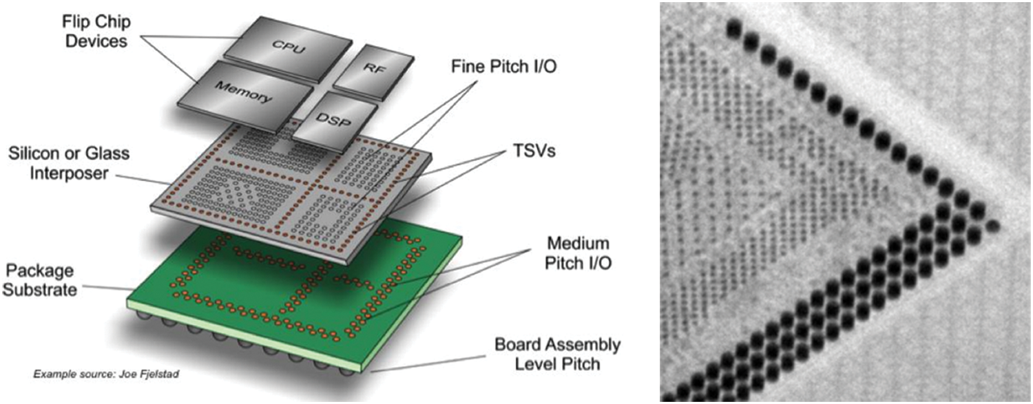
Figure 1: The structure of the multilayer package (left) and its X-ray image (right)
Voids are defects generated inside the solder joint during the reflow process, mainly created by cold joints when insufficient solder is applied to a joint. They might consist of spaces, holes or flux resins inside the solder joint, as shown in Fig. 2.
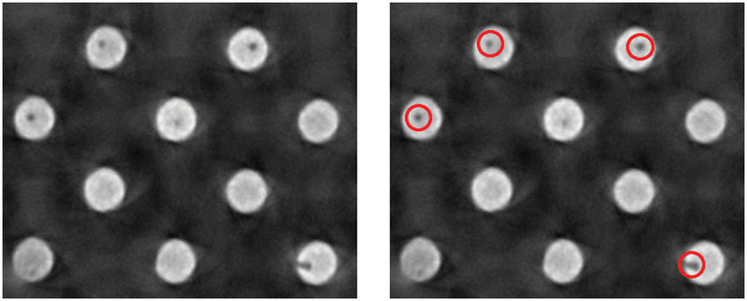
Figure 2: Original X-ray image (left) and the voids (right) in solder balls
The previous automated defect detection methods do not produce good accuracy because a number of challenges exist in 2-D X-ray images. For example, some of these challenges are to find defects, such as voids, cracks, and non-wet defects, in partially and fully occluded situations. The overall X-ray image contrast and brightness can also vary as a function of various devices, PCBs, X-ray operators, etc. The defect detection algorithm needs to cope with all these variations. Aryan et al. [1] reviewed various types of defects, and the capabilities of the most common non-destructive testing methods employed for defect detection. Yuk et al. [2] proposed a non-referential method for fault detection by extracting features based on an image processing method and learning the fault information using random forests. Huang et al. [3] discussed various visual inspection algorithms and systems applied in the semiconductor manufacturing industry. Moreover, they reviewed the multiple defect types of various inspected products that could be referenced for further implementations and improvements.
Image enhancement and segmenting objects in X-ray images have been essential research topics in computer vision concerning defect detection algorithms. Al-Waisy et al. [4] proposed a novel hybrid deep learning system for detecting pneumonia of coronavirus disease of 2019 (COVID-19) in chest X-ray (CX-R) images using two discriminative deep learning approaches. They proposed an effective image enhancement procedure to enhance the CX-R image’s poor quality before feeding to the proposed approaches. Nagi et al. [5] proposed state-of-the-art deep-learning models, and evaluated the performance of deep-learning models for COVID-19 diagnosis using chest X-ray images from a dataset. Hasoon et al. [6] proposed a method for the classification and early detection of COVID-19 through image preprocessing of X-ray images. Kim et al. [7] proposed a new method for real-time anomaly detection in packaged food products using a supervised deep learning network. Park et al. [8] proposed a multi-task learning method that simultaneously learned the lung region and nodule-labeled data based on prior knowledge. Luo et al. [9] presented a comprehensive survey on surface defect detection technologies by reviewing about 120 publications over the last two decades for three typical flat steel products. Liu et al. [10] proposed an improved k-nearest neighbor (KNN) outlier detection algorithm to reduce the time complexity, and improve the performance of anomaly detection. Kim et al. [11] proposed methods for detecting abnormal images on chest X-ray images based on existing anomaly detection techniques.
For the past several years, many methods to segment the solder balls have been proposed, and the most common methods are based on threshold segmentation. The key to threshold segmentation is to find an appropriate threshold. Said et al. [12–15] proposed a way based on the histogram of images. The histogram of the two cluster regions can be represented using a mixture of two Gaussian distributions with two different means and variance parameters. After the segmentation, the major features of principal axis, roundness, and area are used to extract the best candidate solder ball template in the image. This method works well if the background is clean. Nuanprasert et al. [16] proposed a method based on Hough circle detection and Delaunay triangulation. These methods can accurately extract the target solder in images with simple backgrounds. Teramoto et al. [17,18] proposed a novel automated solder inspection technique using oblique computed tomography (OCT). This technique consists of position adjustment, bump extraction, character extraction, and judgment. Linear discriminant analysis and an artificial neural network were proposed as the determination techniques for the automated inspection of BGA soldering. However, it takes a long time to inspect the defects using OCT.
In this paper, to solve these problems, we present a new and fast hybrid inspection algorithm to improve the accuracy of automatic ball segmentation and defect detection of occluded solder balls. Our algorithm consists of two stages. In the first stage, the voids and void candidates are determined using the following four steps: (i) image preprocessing such as noise removal, contrast enhancement, binarization, connected component and morphology, etc., (ii) reducing the inspection area to the ball regions and determining whether the regions are occluded, (iii) segmenting each ball region into one or more regions of similar gray value, and (iv) determining whether there are defects or defective candidates in the regions using a weighted sum of local threshold on local variance. If there are defective candidates, the determination of defects is finally made in the following stage. If defective candidates are not found, the inspection process is finished in the first stage. In the second stage, we confirm the presence or absence of defects using the automated inspection technique based on OCT. The 3D precision computed tomography (CT) inspection process is divided into four steps: (i) obtaining 360 projection images (one image per degree) rotating the object from 0 to 360 degrees, (ii) reconstructing a 3d scene from the 360 images, (iii) finding the center slice of gravity for solder balls from the axial slice images in the z-direction and set the inspection intervals between upper and lower bounds based on the center slice, and (iv) finally determine whether there are voids in the solder ball area using a weighted sum of local threshold on local variance. The main contribution of the proposed hybrid algorithm is to accurately segment the ball regions of the partially occluded solder balls and detect defects quickly. Experimental results show an accuracy of more than 97%.
The rest of this paper is organized as follows: we describe a hybrid automated defect detection algorithm in Section 2. The experimental results and performance of our algorithm are described in Section 3. Lastly, we give our conclusions in Section 4.
2 Hybrid Automated Defect Detection
Since the power of an X-ray tube beam varies, and the thickness of the solder ball and PCB is also changeable, a fixed one-setting level of binarization to the X-ray image of the PCB and package cannot apply to different PCBs and packages. These days, multilayer and double-sided PCBs are used in most electronic devices. The images obtained from X-ray devices for these PCBs are non-occluded, partially occluded, and fully occluded, as shown in Fig. 3. Also, a poor contrast of BGA and the ball’s surrounding background are not homogeneous. Accordingly, it can be a very time-consuming task to detect the voids of each solder ball.
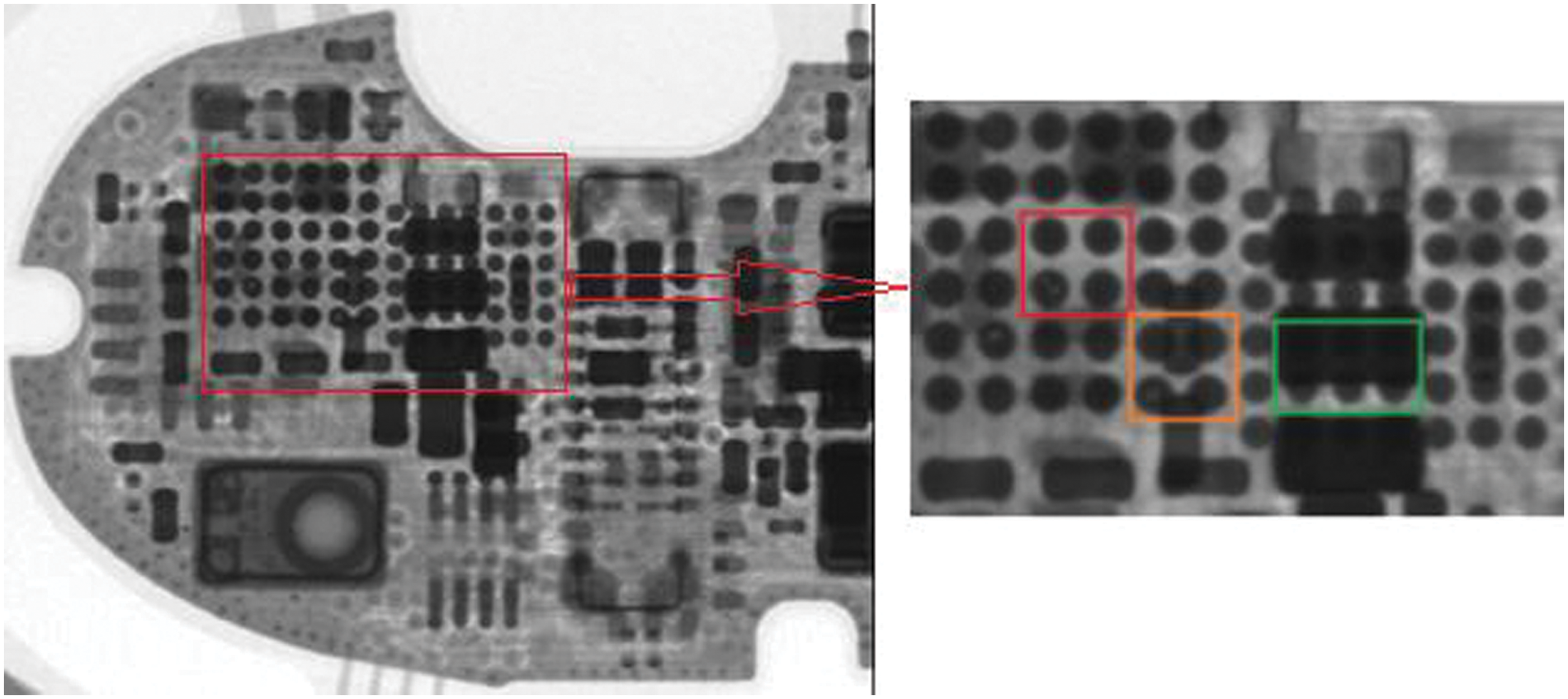
Figure 3: Non-occluded, partially-occluded and fully-occluded solder balls
In this paper, we present a hybrid inspection algorithm that efficiently segments solder balls and detects defects, as shown in Fig. 4. The proposed algorithm consists of two stages: (i) 2D inspection algorithm, and (ii) 3D precision CT inspection algorithm. We find defects or defective candidates using the confidence degree in the first stage. If the confidence degree is greater than
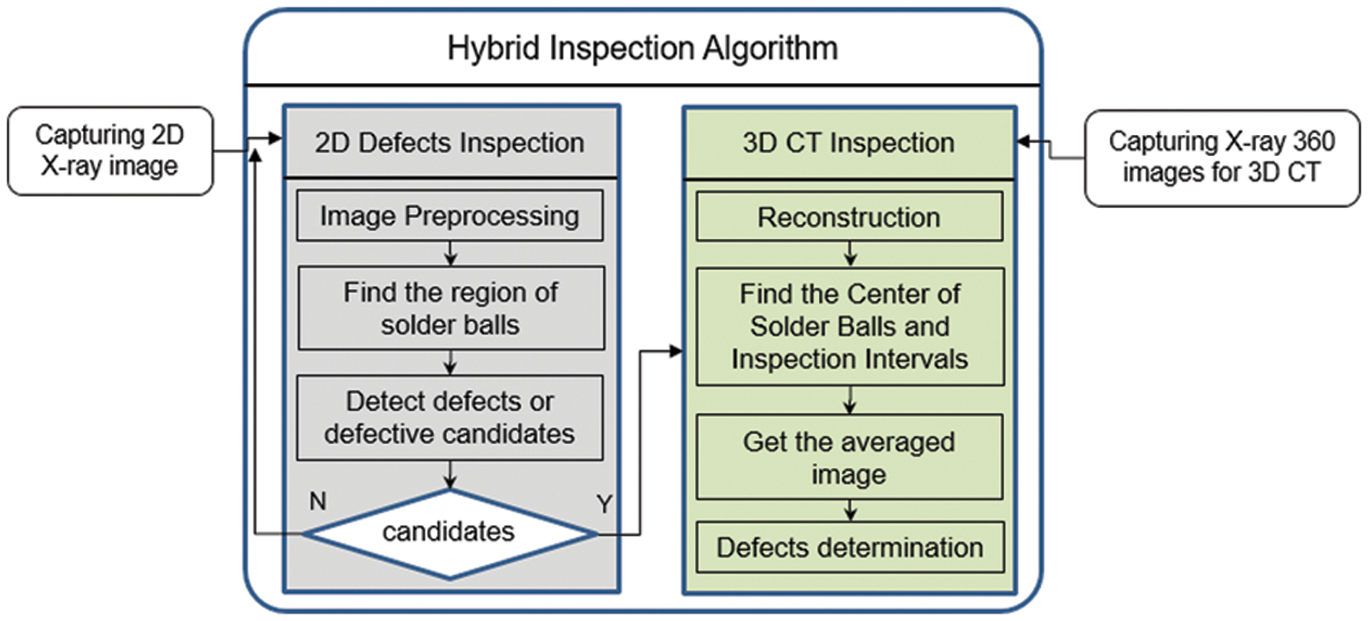
Figure 4: Overview of the proposed hybrid inspection algorithm
In the first stage, the defective candidates or defects are determined using the following four steps: (i) image preprocessing such as noise removal, contrast enhancement, binarization, connected component, and morphology, (ii) reducing the inspection area to the ball regions, and determining whether the regions are occluded, (iii) segmenting each ball region into one or more regions of similar gray value, and (iv) determining whether there are defects or defective candidates in the regions.
The contrast and brightness of the overall X-ray image depend on various devices, PCBs, and X-ray operators. Some regions of the image can be lighter or darker than others. It is necessary to keep the image quality consistent. The contrast enhancement is also used to improve the performance of succeeding tasks, such as solder ball segmentation and defect detection. The image preprocessing steps are shown in Fig. 5. First, noises are reduced through a Gaussian filter. Second, image stretching makes accurate and consistent image analysis with fewer errors, and enhance the contrast of the image. Third, the algorithm that clips the histogram at a predefined value and redistributes the probabilities is applied to the images to remove the contrast amplification. Fourth, adaptive histogram equalization is used to enhance the local contrast. Finally, difference of Gaussians (DOG) is used to remove the noise of the image and enhance its edges.
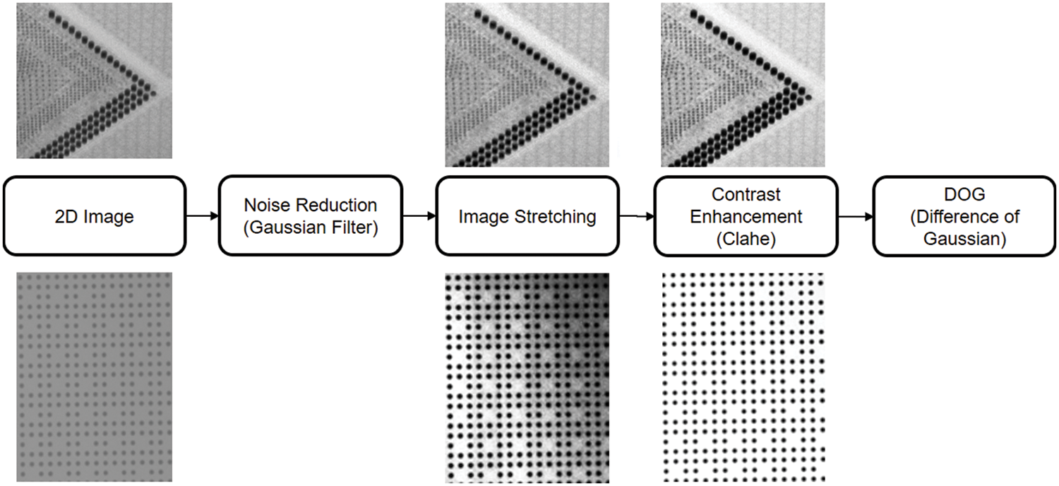
Figure 5: Image preprocessing for the 2D input images
In the second step, an efficient segmentation method for occluded solder ball is presented, as shown in Fig. 6. Otsu’s thresholding method is used for automatic binarization, and all the blobs are segmented. The blobs are labeled using the connected component labeling method. The regions of the blobs are roughly segmented but are refined using closing and opening. We reduce the inspection area to the ball regions, and determine whether the regions are occluded.
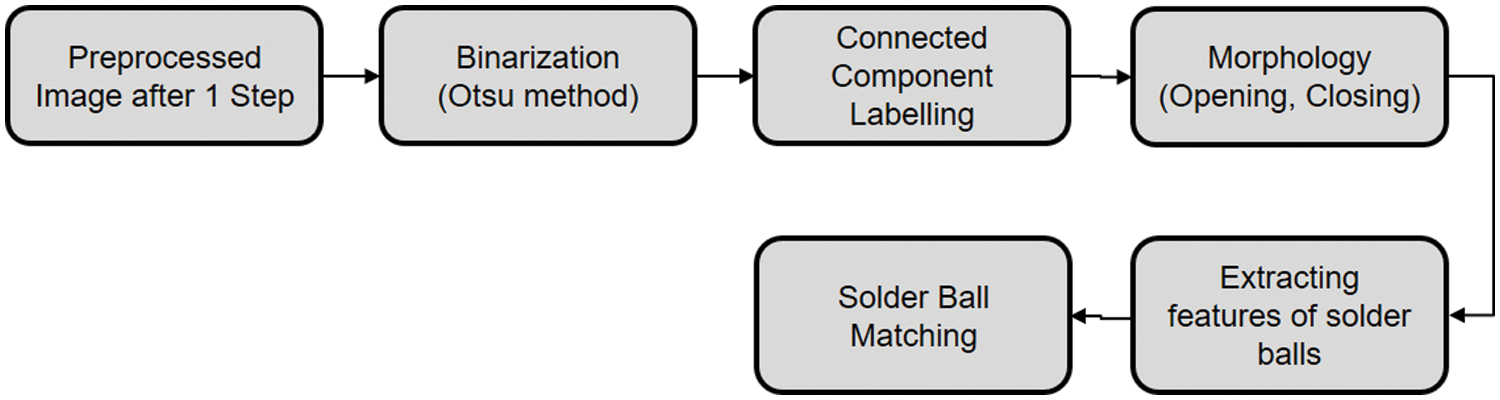
Figure 6: The segmentation process of solder ball after image preprocessing
In the third step, we segment each ball region into one or more regions of similar gray value. The segmentation process of solder balls is completed by eliminating the blobs that are not matched through the feature matching method. The representative features used in feature matching are area, circularity, convexity, etc. The circularity and convexity indicate the degree of similarity to a circle.
In the fourth step, an efficient method to detect the void defects for solder balls is presented. In automatic defect detection, a histogram-based analysis is used to segment defects from a ball region efficiently. In general, if a solder ball and a defect have two distinct peaks, the segmentation of the defect from the solder ball will work quite well. However, when the dynamic histogram range of the ball and defect is narrow, and the segmentation is sensitive to a threshold, the defect detection results vary dynamically. To efficiently segment the defects even in these situations, we use a weighted sum of local thresholds on local variance. A high variance in a local area indicates a more probable region containing void defects in the ball. The best threshold in Eq. (1) is defined as a weighted sum of N small local regions of N×N pixels by dividing the ball.
The each region of the solder balls is masked, and the image area of each masked region is stretched. Then, the first general local binarization process for each masked image area is performed, and the second binarization threshold using optimal threshold by local variance is performed. The union process of the two images obtained through the two binarization processes is performed, and the void regions are segmented, as shown in Fig. 7. The segmented regions are enlarged and reduced through morphological opening and closing. If the confidence C(i) in Eq. (2) is greater than a predefined threshold, the union of the regions in the solder ball is determined as a defect or a defective candidate. If defective candidates are not contained in the solder balls, only 2D inspection is performed. Otherwise, the defect determination for the candidates is done in the following CT inspection stage.
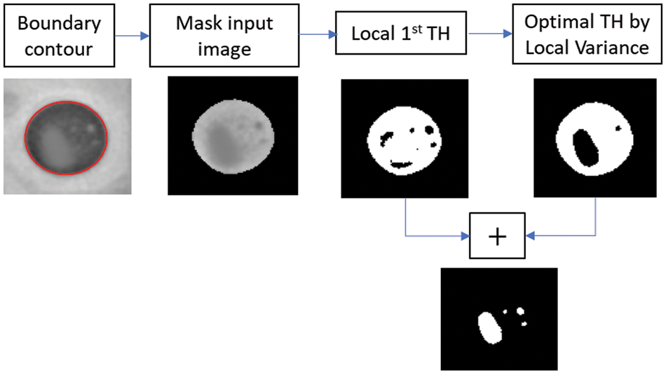
Figure 7: Optimal threshold as a weighted sum of local variance
where
In the second stage, we confirm the presence or absence of defects for the defective candidates using the automated inspection technique based on OCT. The 3D precision CT inspection process is divided into four steps: (i) obtain 360 projection images rotating the object from 0 to 360 degrees, (ii) reconstruct a 3D scene from the 360 images, (iii) find the center slice of gravity,
After reconstructing a 3D scene from 360 images, we find the center of gravity of solder balls,
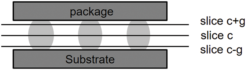
Figure 8: The center slice of gravity and inspection bounds for solder balls in the z-direction
l(k) is the total number of blobs,
n is the total number of cross-sectional images in the z-direction
Eq. (3) is used to find the slice k,
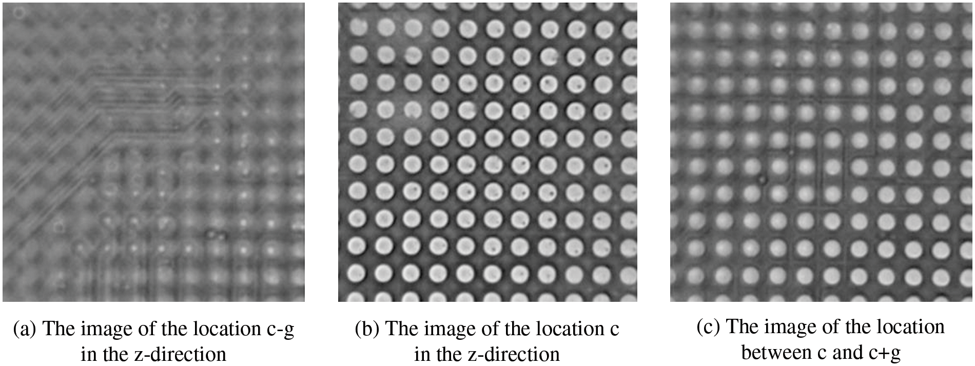
Figure 9: Three cross-sectional images for locations in the z-direction
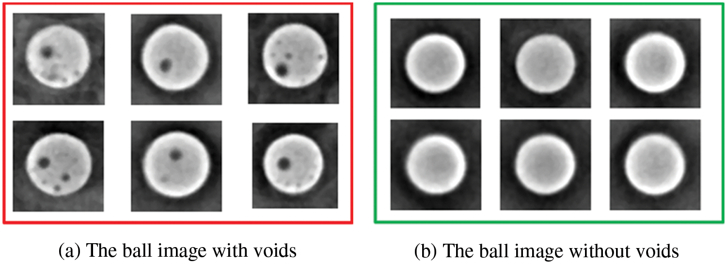
Figure 10: Averaged images in the z-direction obtained by averaging the slice images between c−g and c+g
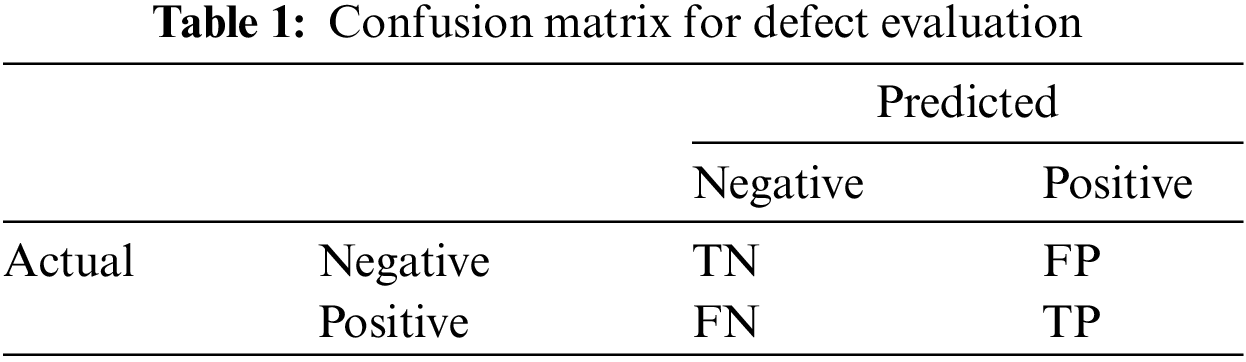
Finally, we determine whether there are voids in the solder ball regions of the averaged image. The voids in the averaged image are detected using the same 2D defect inspection method presented in the previous chapter. The defects can be easily detected in these CT images of good quality, as shown in Fig. 10. To evaluate the performance, we use Precision, Recall, Accuracy, and F1-score using TP (True Positive), TN (True Negative), FN (False Negative), FP (False Positive), as shown in Table 1. TP is the number of the good solder balls that are correctly classified, TN is the number of the defective solder balls that are correctly classified, FN is the number of the good solder balls that are incorrectly classified, and FP is the number of the defective solder balls that incorrectly classified. The precision is the number of TP divided by the total number of solder balls detected as belonging to the positive class. Recall is the number of TP divided by the total number of the solder balls that belong to the positive class. The accuracy is defined by (TP+TN)/(TP+TN+FP+FN), and F1-score is defined by 2 * (precision * recall)/(precision+recall).
To evaluate the performance of our algorithm, a hybrid inspection algorithm was performed using a BGA substrate and package in which soldering defects occurred, as shown in Fig. 11. The number of solder balls in the PCB was more than 1000, and all solder balls were classified as good or defective by manually viewing the OCT images. We selected ten partially occluded solder balls with voids and ten partially occluded solder balls without voids, as shown in Fig. 13, and then we experimented 100 times on a X-ray device. However, we did not have an experiment that segments two and more solder balls in 70% or more partially occluded conditions. We selected five insufficient solder balls and five excessive solder balls, as shown in Fig. 13, and then we experimented 40 times. The experiment was performed using a 2D+3D hybrid inspection system. Moreover, the overall X-ray image contrast and brightness can vary as a function of various devices and operators. To evaluate measurement variation in these situations, we experimented on the two X-ray devices using the same voltage and electric current.
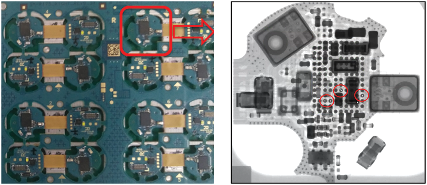
Figure 11: BGA substrate (left) used for the experiment and the X-ray image with voids (right)
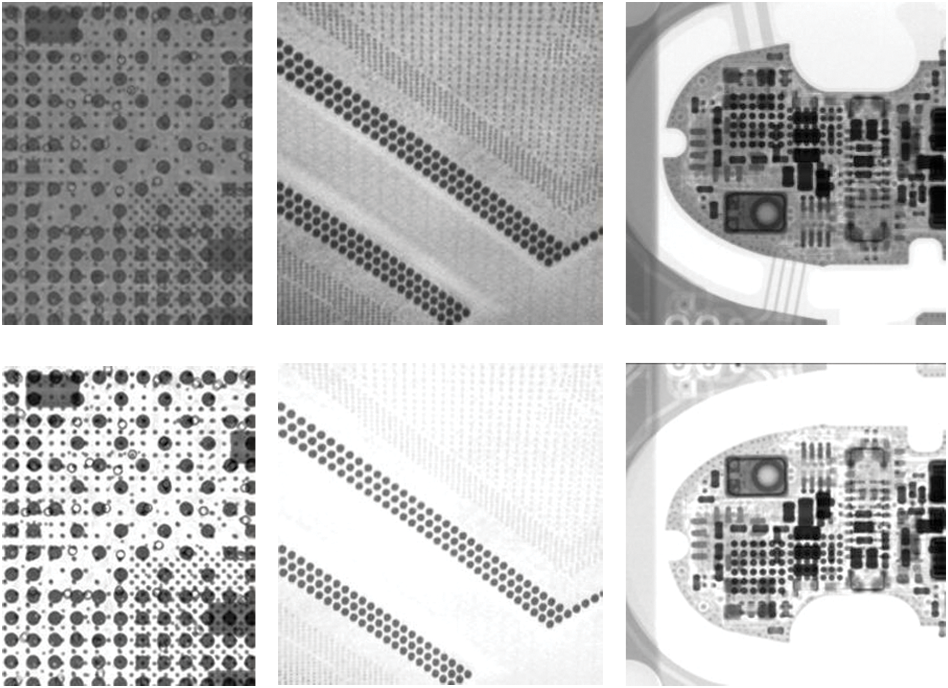
Figure 12: The input image before preprocessing (up) and the image after preprocessing (down)
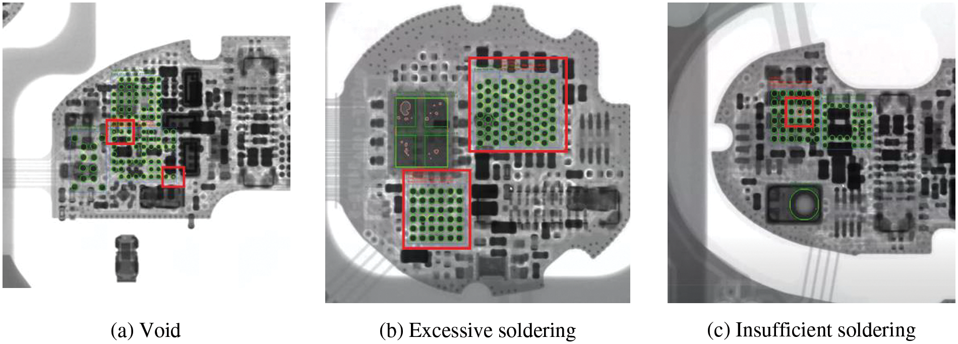
Figure 13: Defects used in the experiment
In the first stage, we preprocessed the image to improve the performance of succeeding tasks, such as solder ball segmentation and defect detection. The image preprocessing for the 2D input images was performed, as shown in Fig. 12. Noise removing was done by convolving an image with the Gaussian filter of a 5 × 5 kernel size. We enhanced and adjusted the contrast of an image that was not homogenous with histogram stretching and contrast limited adaptive histogram equalization (CLAHE). The clip limit of CLAHE is set to 0.01. Then, we blurred and removed the noise with Gaussian filter of two kernel sizes (3 × 3, 7 × 7), and the sigma of the DOG filter was set to 1.0.
In the following steps, we had the experiments to segment the regions of occluded solder balls and detect defects in the regions. First, we used otsu’s thresholding method for automatic binarization-level decisions based on the shape of the histogram. Second, all components in images were detected and labeled using the connected component labeling method. Third, the regions and their edges of the components were refined using closing and opening. Some regions for all components were eliminated through the features matching method. We reduced the inspection area to the ball regions, and determined whether the solder balls in the regions were occluded. We then segmented each ball region into one or more regions of similar gray value. Finally, we determined whether there were defects or defective candidates in the regions using a weighted sum of local thresholds on local variance. The union of regions in ith solder ball was determined as a void defect if it satisfied the condition that the C(i) was greater than the predefined threshold, which was set to 10%. The union of regions in ith solder ball was determined as a void candidate if it satisfied the condition that the C(i) was greater than the predefined threshold, which was set to 5%. If C(i) is less than 5%, a void does not exist in the ith solder ball. The union of the region contained in the 1st solder ball was greater than 10%, as shown in Fig. 14b, so it was determined as a void. However, the union of void regions contained in the 2nd solder ball was less than 10%, so it was determined as a void candidate. The defective candidates could be classified as defects in the following stage.
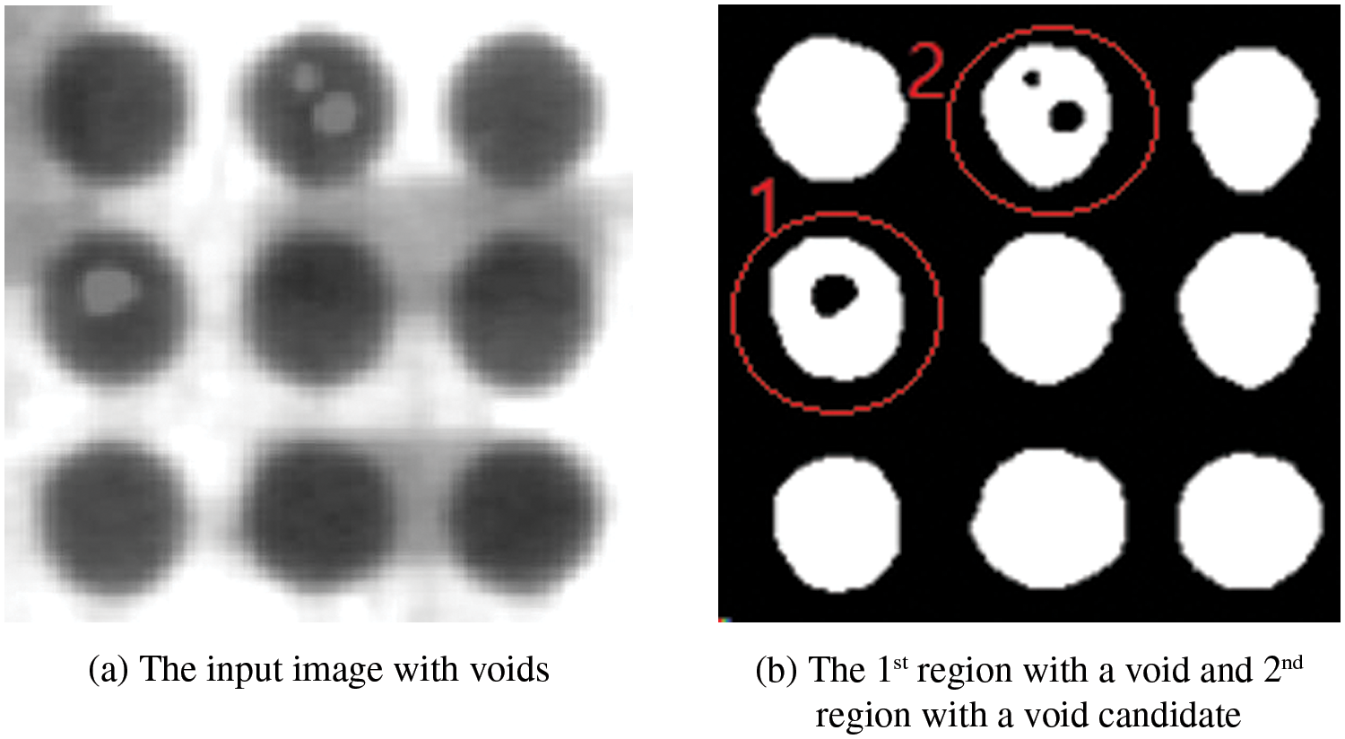
Figure 14: The input image and binarized image with voids
The 3D image was reconstructed using 360 projection images, and the pitch angle for the projection was 1 degree. By parallelizing the collection of the projection images, reconstruction processing and inspection of the defects, the 3D inspection was completed in 4 s.
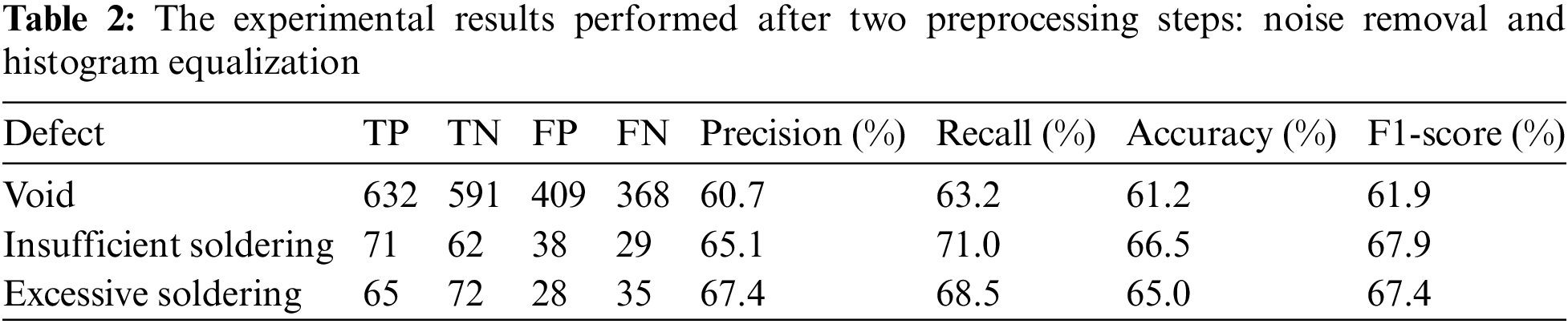
To evaluate the performance, we used TP, TN, FN, FP, Precision, Recall, Accuracy and F1-score. The first experiment was performed after only two preprocessing steps: noise removal and histogram equalization. The results are shown in Table 2. The precision value, recall value, accuracy and F1-score for void defects were less than 64.0%. The precision value, recall value, accuracy and F1-score for insufficient soldering were less than and equal to 71.0%. The precision value, recall value, accuracy and F1-score for excessive soldering were less than 69.0%.
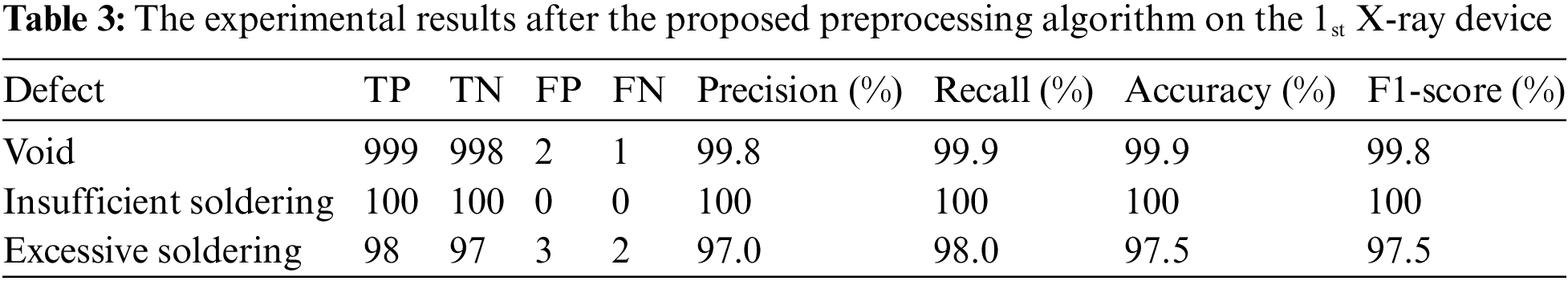
The second experiment was performed on the 1st X-ray device using the proposed preprocessing algorithm. The results are shown in Table 3. The precision value, recall value, accuracy and F1-score for void defects were above 99.8%. The precision value, recall value, accuracy and F1-score for insufficient soldering were 100%. The precision value, recall value, accuracy and F1-score for excessive soldering were above 97.0%.
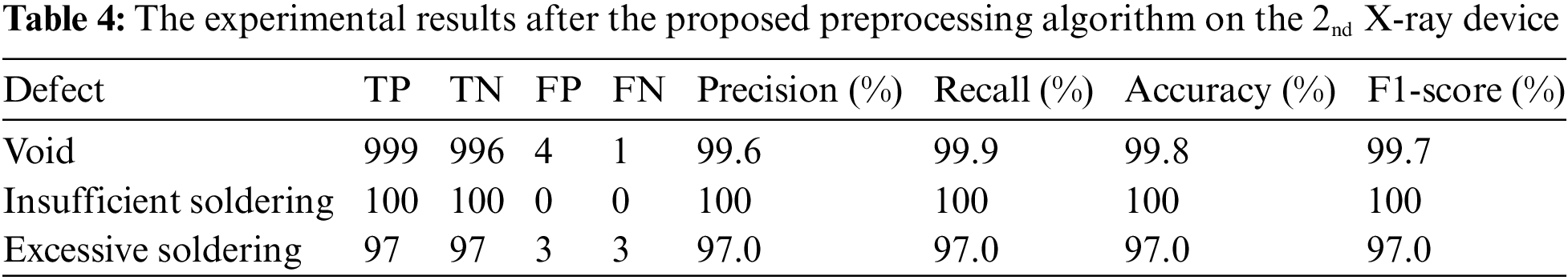
The third experiment on the 2nd X-ray device was performed under the same voltage and electric current as the second experiment. The results are shown in Table 4. The precision value, recall value, accuracy and F1-score for void defects were above 99.6%. The precision value, recall value, accuracy and F1-score for insufficient soldering were 100%. The precision value, recall value, accuracy and F1-score for excessive soldering were above 97.0%.
In this paper, we presented a new hybrid automatic inspection algorithm that segmented solder balls and detected defects efficiently when solder balls were occluded. The proposed algorithm consists of two stages. In the first stage, we determined the defective candidates or defects using the following four steps: image preprocessing, determining whether the regions are occluded, segmenting each ball region into one or more regions, determining whether there are defects or defective candidates in the regions using a weighted sum of local threshold on local variance. If there were defective candidates, the determination of defects was finally made in the next stage. In the second stage, we detected defects using the automated inspection methodology based on OCT. The OCT inspection process was divided into four steps: obtaining 360 projection images, reconstructing a 3d scene, finding the center slice of gravity for solder balls and getting the inspection intervals from the center slice, and finally determining whether there are defects in the averaged image of solder balls.
To evaluate the performance of our hybrid algorithm, we had two experiments. The first experiment was performed after only the two preprocessing: noise removal and histogram equalization. The precision value, recall value, accuracy, and F1-score for void defects were less than 64.0%. The precision value, recall value, accuracy, and F1-score for insufficient soldering were less than and equal to 71.0%. The precision value, recall value, accuracy and F1-score for excessive soldering were less than 69.0%. The second experiment was performed on the 1st X-ray device and 2nd X-ray device using the proposed preprocessing algorithm. The precision value, recall value, accuracy and F1-score for void defects were above 99.8%. The precision value, recall value, accuracy, and F1-score for insufficient soldering were 100%. The precision value, recall value, accuracy and F1-score for excessive soldering were above 97.0%.
We had the limitation that we did not have an experiment that segments solder balls in 70% or more partially occluded conditions. It is still difficult to accurately segment the regions of occluded solder balls. Also, we did not apply our proposed algorithm to detecting other types of defects. We will apply our algorithms to defects such as non-wet, short, and head in pillow (HIP) that may occur in PCBs and packages.
Funding Statement: The authors received no specific funding for this study.
Conflicts of Interest: The authors declare that they have no conflicts of interest to report regarding the present study.
References
1. P. Aryan, S. Sampath and H. Sohn, “An overview of non-destructive testing methods for integrated circuit packaging inspection,” Sensors, vol. 18, no. 7, pp. 1981–2018, 2018. [Google Scholar] [PubMed]
2. E. Yuk, S. Park, S. Park and J. -G. Baek, “Feature-learning-based printed circuit board inspection via speeded-up robust features and random forest,” Applied Science, vol. 8, no. 6, pp. 932–945, 2018. [Google Scholar]
3. S. -H. Huang and Y. -C. Pan, “Automated visual inspection in the semiconductor industry: A survey,” Computers in Industry, vol. 66, no. 6, pp. 1–10, 2015. [Google Scholar]
4. A. Al-Waisy, M. Mohammed, S. Al-Fahdawi, M. Maashi, B. Garcia-Zapirain et al., “COVID-DeepNet: Hybrid multimodal deep learning system for improving covid-19 pneumonia detection in chest X-ray images,” Computers, Materials & Continua, vol. 67, no. 2, pp. 2409–2429, 2021. [Google Scholar]
5. A. Nagi, M. Awan, M. Mohammed, A. Mahmoud, A. Majumdar et al., “Performance analysis for COVID-19 diagnosis using custom and state-of-the-art deep learning models,” Applied Science, vol. 12, pp. 6364–6387, 2022. [Google Scholar]
6. J. Hasoon, A. Fadel, R. Hameed, S. Mostafa, B. Khalaf et al., “COVID-19 anomaly detection and classification method based on supervised machine learning of chest X-ray images,” Results in Physics, vol. 31, no. 1, pp. 105045, 2021. [Google Scholar] [PubMed]
7. K. Kim, H. Kim, J. Chun, M. Kang, M. Hong et al., “Real-time anomaly detection in packaged food X-ray images using supervised learning,” Computers, Materials & Continua, vol. 67, no. 2, pp. 2547–2568, 2021. [Google Scholar]
8. S. Park, W. Jeong and Y. S. Moon, “X-ray image segmentation using multi-task learning,” KSII Transactions on Internet and Information Systems, vol. 14, no. 3, pp. 1104–1120, 2020. [Google Scholar]
9. Q. Luo, X. Fang, L. Liu, C. Yang and Y. Sun, “Automated visual defect detection for flat steel surface: A survey,” IEEE Transactions on Instrumentation and Measurement, vol. 69, no. 3, pp. 626–644, 2020. [Google Scholar]
10. X. Liu, J. Ren, H. He, Q. Wang and S. Sun, “A novel network anomaly detection method based on data balancing and recursive feature addition,” KSII Transactions on Internet and Information Systems, vol. 14, no. 7, pp. 3093–3115, 2020. [Google Scholar]
11. H. -B Kim and J. -C Chun, “Leision detection in chest X-ray images based on coreset of patch feature,” Journal of Internet Computing and Services, vol. 23, no. 3, pp. 35–45, 2022. [Google Scholar]
12. A. F. Said, B. L. Bennett, L. J. Karam, A. Siah, K. Goodman et al., “Automated void detection in solder balls in the presence of vias and other artifacts,” IEEE Transactions on Components, Packaging and Manufacturing Technology, vol. 2, no. 11, pp. 1890–1901, 2012. [Google Scholar]
13. A. F. Said, B. L. Bennett, L. J. Karam and J. S. Pettinato, “Automated detection and classification of non-wet solder joints,” IEEE Transactions on Automation Science and Engineering, vol. 8, no. 1, pp. 67–80, 2011. [Google Scholar]
14. A. F. Said, B. L. Bennett, F. Toth, K. J. Lina and P. Jeff, “Non-wet solder joint detection in processor sockets and BGA assemblies,” in Proc. IEEE Electronic Components and Technology Conf., Las Vegas, USA, pp. 1147–1153, 2010. [Google Scholar]
15. A. F. Said, B. L. Bennett, L. J. Karam and J. Pettinato, “Robust automatic void detection in solder balls,” in Proc. IEEE Int. Conf. on Acoustics, Speech and Signal Processing, Dallas, USA, pp. 1650–1653, 2010. [Google Scholar]
16. S. Nuanprasert, S. Baba and T. Suzuki, “An efficient method of occluded solder ball segmentation for automated BGA void defect inspection using X-ray images,” in Proc. IEEE Industrial Electronics Society, Yokohama, Japan, pp. 3308–3313, 2015. [Google Scholar]
17. A. Teramoto, T. Murakoshi, M. Tsuzaka and H. Fujita, “Automated solder inspection technique for bga-mounted substrates by means of oblique computed tomography,” IEEE Transactions on Electronics Packaging Manufacturing, vol. 30, no. 4, pp. 285–292, 2007. [Google Scholar]
18. A. Teramoto, T. Murakoshi, M. Tsuzaka and H. Fujita, “Automated solder inspection method by means of X-ray oblique computed tomography,” in Proc. IEEE Int. Conf. on Image Processing, San Antonio, USA, pp. 433–436, 2007. [Google Scholar]
Cite This Article
 Copyright © 2023 The Author(s). Published by Tech Science Press.
This work is licensed under a Creative Commons Attribution 4.0 International License , which permits unrestricted use, distribution, and reproduction in any medium, provided the original work is properly cited.
 Downloads
 Citation Tools