
 Submit a Paper
 Propose a Special lssue
 Open Access
ARTICLE

A Flexible Architecture for Cryptographic Applications: ECC and PRESENT
1 Department of Computer Engineering, Umm Al-Qura University, Makkah, 21955, Saudi Arabia
2 Computer Science Department, Umm Al-Qura University, Makkah, 21955, Saudi Arabia
3 Cyber R&D Specialist, NASTP, Rawalpindi, 46000, Pakistan
4 Department of Information Systems, Umm Al-Qura University, Makkah, 21955, Saudi Arabia
* Corresponding Author: Muhammad Rashid. Email:
Computers, Materials & Continua 2023, 76(1), 1009-1025. https://doi.org/10.32604/cmc.2023.039901
Received 23 February 2023; Accepted 20 April 2023; Issue published 08 June 2023
 View Full Text
 Download PDF
Abstract
This work presents a flexible/unified hardware architecture of Elliptic-curve Cryptography (ECC) and PRESENT for cryptographic applications. The features of the proposed work are (i) computation of only the point multiplication operation of ECC over for a 163-bit key generation, (ii) execution of only the variant of an 80-bit PRESENT block cipher for data encryption & decryption and (iii) execution of point multiplication operation (ECC algorithm) along with the data encryption and decryption (PRESENT algorithm). To establish an area overhead for the flexible design, dedicated hardware architectures of ECC and PRESENT are implemented in the first step, and a sum of their hardware area is computed. Then, the implementation of the proposed flexible architecture for ECC and PRESENT algorithms is presented. Implementation results regarding the area, clock cycles, latency, clock frequency, and power after the place-and-route level on Xilinx Virtex-5, Virtex-6, and Virtex-7 FPGA devices are presented. Hence, the implementation results and comparisons show that the proposed architecture suits applications demanding flexible implementation of cryptographic applications.Keywords
In the last few years, we have witnessed a massive increase in the use of embedded devices, such as the automatic control of electronic appliances and smart cards for electronic payments [1]. It has been observed that the desired features/attributes for these application-specific embedded devices include low power consumption, limited memory usage (area), reasonable performance, and flexibility [2]. In addition, security is another critical demand for these devices [2,3]. Comparatively, the symmetric cryptographic algorithms are beneficial to obtain low power, limited area, and high performance as compared to public-key cryptographic (PKC) algorithms. On the other hand, the PKC algorithms are prevalent for higher security achievement. Hence, one of the alternatives for the security improvement of application-specific embedded devices is to unify the advantages of symmetric and PKC algorithms; this unification specifies flexibility which is a critical need of application-specific embedded devices and is a means of interest in this work.
Several applications demand flexible cryptographic implementations. Examples are online banking payments by smart cards, where for each transaction, a unique secret key is required to complete the computation [4]. Another example includes identity-based public key cryptography, where a trusted third party (or the private key generator) generates a public key to affirm a specific device on the network [5]. Also, blockchain technology requires separate keys or digital signatures for secure communications such as online payments, tracking orders, maintaining business accounts, and many more online transactions. In this regard, in 2022, a blockchain-based reliable, and efficient certificateless signature scheme is presented in [6] for securing industrial internet of things devices. Hence, these applications confirm the need for a flexible cryptographic system that allows the generation of separate keys for each encryption and decryption operation. This motivates us to implement such a system that covers today’s needs.
The National Institute of Standards and Technology (NIST) has standardized several symmetric and PKC algorithms/protocols to address the security concerns related to application-specific embedded devices. However, the current symmetric and PKC standards are Advance Encryption Standard (AES), Elliptic Curve Cryptography (ECC) [7], and Rivest-Shamir-Adleman (RSA) [8].
The cryptographic standards/algorithms can be implemented on software (SW) and hardware (HW) platforms. The SW implementations (such as on microcontrollers) provide higher flexibility but offer limited performance and security [3]. On the other hand, the HW implementations, such as field-programmable gate arrays (FPGA) and application-specific integrated circuits (ASICs), provide higher processing speed/performance but with limited flexibility [2,3]. More precisely, unlike the ASIC implementations, FPGA devices offer flexibility due to a re-configurability feature but are not comparable to pure SW-implemented designs. Therefore, an FPGA platform is preferred in this study to obtain a flexible cryptographic hardware accelerator with a focus on higher performance. This is the objective of this work.
1.1 Motivation for Selecting PRESENT and ECC Algorithms
Concerning [9,10], the excessive hardware resource utilization makes the existing symmetric standard (i.e., AES algorithm) ineffective for the area-constrained applications compared to the PRESENT block cipher. Therefore, we have preferred PRESENT block cipher for encryption/decryption over data in our implementation.
For PKC, ECC has become a promising approach to securing internet-of-things (IoT) and smart-card and securely generating digital signatures because it offers an equivalent security level with shorter key lengths than the RSA algorithm [11–13]. Moreover, ECC requires low hardware resource utilization and power consumption without reducing security than RSA; hence, the former is beneficial to secure low-power and low-memory resource-constrained IoT devices. Additionally, by offering a shared key mechanism for the wireless sensor nodes connected to the IoT infrastructures in the networks, it prevents unauthorized appliances from acquiring a permit for wireless sensor networks (WSNs) [14,15]. Moreover, an ECC-based Diffie Hellman protocol [16] allows the generation of a shared key for security-related systems. According to [17,18], ECC could be more beneficial in satisfying security challenges related to radio-frequency identification (RFID) technologies. In addition, ECC-based RFID authentication protocols are employed in intelligent healthcare environments to enhance medical data security [19]. ECC-based digital signature schemes are adopted in wireless body area networks (WBANs) to satisfy the security needs for real-time health data management [20]. Hence, the scenario presented above declares that ECC is widely adopted for securing range of cryptographic applications. Therefore, based on this compliance, we have selected ECC for key generation in our flexible design.
1.2 Related Hardware Accelerators and their Limitations
For addressing the data security issues, the cryptographic algorithms (symmetric and asymmetric/public-key) are (frequently) demonstrated in literature as hardware accelerators on FPGA and ASIC platforms. A lightweight RECTANGLE symmetric cipher is implemented in [21] for data encryption and decryption on wireless sensor nodes. For similar encryption and decryption on wireless sensor nodes, a co-design of AES is implemented in [22] on hardware (180 nm and 90 nm process technologies) and software (microcontrollers) platforms. A SIMON block cipher is implemented in [23] for securing low-resource embedded devices. Specific to IEEE 802.15.4 standard, a SIMECK32/64 block cipher is implemented in [24]. For securing low resource-constrained applications, three dedicated hardware architectures are presented in [25] for three lightweight cryptographic algorithms, i.e., LED64/128, SIMON64/128, and SIMECK64/128. ASIC demonstration of HIGHT and PRESENT block ciphers is provided in [26].
Hardware accelerators of [2,27,28] reveal that flexible cryptographic designs are (also) known in the literature to secure embedded devices where the benefits of symmetric and PKC algorithms are combined/unified. The design of [2] presents a unified architecture to integrate AES and ECC. Similarly, a dual-field ECC processor combined with AES is shown in [27]. Recently, in 2018, a compact co-processor architecture of ECC and AES for IoT devices has been described in [28].
The state-of-the-art implementations show that the symmetric algorithms are more beneficial regarding resource utilization and consumed power. However, the requirement of key storage inside the embedded devices is one of the significant limitations. On the other hand, asymmetric algorithms do not require key storage; however, these are area and power-hungry [3,13,15]. Similarly, the unified hardware accelerators of AES and ECC [2,27,28] are specific to key generation using ECC and encryption & decryption by employing AES; this is only the benefit of the flexible designs of [2,27,28]. We believe it is possible to obtain some more benefits by setting architecture(s) with the following key features: (i) only the computation of key generation, (ii) only the execution of encryption & decryption processes, and (iii) the computation of both key generations followed by encryption & decryption operations. This requires only an efficient control logic without the additional arithmetic blocks (of an adder, multiplier, and square) for PRESENT and ECC algorithms. Additionally, the flexible state-of-the-art designs of [2,27,28] utilize higher hardware resources and consume more power. Like flexibility, other critical parameters, i.e., hardware resources (area) and consumed power, can be improved by employing different architectural strategies.
Therefore, we present our novel contributions to address the aforementioned security issues below.
• Flexible accelerator architecture: We have proposed a flexible (or unified) hardware architecture of ECC and PRESENT algorithms with three different compositions, (i) execution of only a 163-bit key generation using ECC, (ii) only the execution of encryption and decryption using an 80-bit PRESENT block cipher, and (iii) execution of the key generation of ECC with a variant of a PRESENT block cipher for data encryption & decryption.
• Strategies for area and power optimizations: We have realized a shift-and-add multiplier in the ECC-based key generation architecture. The square operations for ECC implementations are computed by providing identical inputs to our utilized shift-and-add multiplier. For inverse computations, we also used the existing hardware resources of our shift-and-add multiplier. These techniques allow us to reduce hardware costs. Moreover, the design of our shift-and-add multiplier is a bit-serial. Therefore, it consumes very low power.
• Dedicated controller: A finite-state-machine (FSM) based dedicated controller is presented to implement three different compositions of our flexible design. More insight details are given in Section 3.4.
• Dedicated designs for ECC and PRESENT: Dedicated architectures for both ECC and PRESENT algorithms are implemented to establish an area overhead for the proposed unified design.
The proposed hardware designs are implemented in Verilog HDL using the Vivado IDE tool and reported implementation results on Xilinx Virtex-5, Virtex-6, and Virtex-7 FPGA devices after the place-and-route level. On modern Virtex-7 FPGA, the total sum of slices for the dedicated design of ECC and PRESENT algorithms is 1.24 times higher than our proposed flexible architecture. The dedicated and flexible hardware designs achieved a maximum clock frequency of 387 MHz (for ECC), 407 MHz (for PRESENT), and 200 MHz (for flexible architecture) on the same Virtex-7 device. Thus, the implementation results and comparison to state-of-the-art reveal that the proposed flexible design is suitable for applications that need flexible cryptographic accelerators. Note that the proposed accelerator design can operate on a 163-bit key length for ECC and an 80-bit key size for PRESENT. As the block size of the PRESENT cipher is 64, this means that our accelerator can encrypt and decrypt only 64-bit message size at one time.
The remainder of this work is structured as follows: Section 2 provides the related background for PM computation of ECC and PRESENT algorithm. Our proposed architecture is described in Section 3. The implementation results are given in Section 4. Finally, Section 5 concludes the paper.
2.1 Elliptic Curve Cryptography
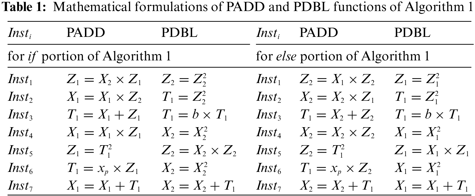
The ECC includes four layers of operations [11,13]. The uppermost protocol provides encryption/decryption and signature generation/verification. The most crucial process to compute in ECC is point multiplication (PM), and it relies on the implementation of point addition (PADD) and double (PDBL) operations (these are layer two operations of ECC). Each PADD and PDBL computation depends on the execution of finite field arithmetic operations, i.e., addition, multiplication, square, and inversion.
ECC include prime and binary finite fields [11].
In Eq. (1),
In Eq. (2),
In Eq. (3),

PRESENT is a lightweight block cipher having a block size of 64 bits. It supports 80 and 128-bit key lengths. The structure of the PRESENT block cipher depends on the computation of AddRoundKey, substitution, and permutation operations. It includes 32 rounds to perform the desired crypto operations (encryption and decryption). For the initial 31 rounds, substitution and permutation operations are essential to execute after the computation of AddRoundKey. For the final round, we need only the AddRoundKey process to perform. We direct readers to [31] for complete mathematical descriptions.
3 Proposed Flexible Architecture
There are various ways to establish a flexible architecture for cryptographic applications that involve ECC and PRESENT algorithms. One approach uses a co-processor method, where ECC and PRESENT algorithms drive on hardware while software processors manage other blocks. Indeed, this approach provides higher flexibility but has limited performance compared to crypto processor designs, where all blocks serve on hardware. We designed an efficient hardware controller to handle our chosen ECC and PRESENT algorithms to achieve flexibility while maintaining high performance. Therefore, we provide the top-level diagram of the proposed approach in Fig. 1. It includes two crypto cores, one for ECC and another for PRESENT, a controller, and a key-transformation unit. The ECC core generates public and private keys, while the PRESENT core performs encryption/decryption over a 64-bit data block. With the help of a controller, a user can generate public and private keys (only executing the ECC block), performs encryption/decryption (utilizing only the PRESENT core), and combine public and private keys followed by encryption/decryption using ECC and PRESENT cores. Key-transformation block generates an 80-bit key from a 163-bit generated by ECC for the PRESENT crypto core. The output of the key-transformation block goes back to the controller for related functionalities.

Figure 1: Overall idea of the proposed approach
We show the detailed visualization of Fig. 1 in Fig. 2. It incorporates four units: (i) a 163-bit key generator architecture using ECC (

Figure 2: Hardware design of the proposed flexible architecture. Note that the green and orange portions are sequential blocks, requiring several clock cycles for computation; conversely, the key-transformation block is combinational as it needs bit manipulations to complete the computation in one clock cycle
As shown in Fig. 2, the KeyGenerator architecture consists of (i) two routing paths, i.e., RoutingPath1 and RoutingPath2, (ii) a storage element of size 5 × 163 and (iii) an arithmetic and logic unit (ALU). We describe these blocks as follows:
3.1.1 RoutingPath1 and RoutingPath2
The RoutingPath1 takes an ECC parameter (xp, yp, & b) and an operand from the memory unit. The xp and yp show the x and y coordinates of the initial point P on the curve. A parameter b is the curve constant. These parameters we have selected from the NIST recommended document of [32]. Similarly, the RoutingPath2 selects the appropriate data incoming from the finite field adder and multiplier units, and its output returns to the memory block.
3.1.2 Memory Unit (
The supported key length for ECC is 163-bit, so the memory block reserves 163-bit data on each memory address. It is essential to identify the total number of memory addresses needed. Therefore, in implementing the Montgomery PM Algorithm 1, a 5 × 163 memory block size is implemented, where numbers 5 and 163 specify the total number of addresses and the length of data stored on each address, respectively. The objective of the memory block is to preserve the intermediate and final results; during the implementation of Montgomery PM Algorithm 1.
3.1.3 Arithmetic and Logic Unit
The ALU comprises an adder and a multiplier unit. As we target binary field ECC in our implementation, implementing an adder is simple than the multiplier block. We implement the adder employing an m-bit array of Exclusive(OR) gates, where m specifies the secret key size (i.e., 163) or a scalar multiplier d. For the binary ECC field, hardware accelerators of [13,29,30] use the same approach to implement an adder. The adder inputs two m-bit operands (OPF1 and OPF2) and outputs one m-bit operand (Aout). Moreover, one m-bit polynomial addition requires one clock cycle. On the other hand, several bit-level & digit-level approaches to accomplish polynomial multiplication in ECC exist. Examples of bit-serial multiplication methods are the schoolbook (SBM) and Booth. Some bit parallel multipliers include Karatsuba and Toom-Cook. Similar to bit-serial and bit-parallel multiplication methods, numerous digit-serial and digit-parallel techniques are also available. It is essential to note that each multiplication method has pros and cons. Thus, the existing multiplication architectures indicate that the bit-serial techniques are widely used for area and power-constrained applications [17]. Bit/digit parallel multiplication architectures are better suited for high-speed cryptographic applications with higher-hardware resources and consumed power [13,27,28]. Using digit-serial multipliers is advantageous for applications that demand high-speed and low-area simultaneously [30]. Therefore, in this work, an SBM multiplier is employed to utilize the minimum hardware area for the multiplier unit. It takes two m-bit operands as inputs and results in an operand of length 2 × m − 1 bit as output. It incorporates shifting (by one bit towards the left) and addition operations. For one polynomial multiplication, the computational complexity of our implemented SBM multiplier is 163 clock cycles, as it operates in a bit-serial fashion. In Fig. 2, a POLRED unit is connected after the MULT unit to reduce a polynomial of length 2 × m − 1 bit to an m-bit polynomial. To perform a polynomial reduction over
Also, we have used the SBM multiplier to compute the square instructions of PADD and PDBL functions (see Table 1) of Algorithm 1 for ECPM implementation. We achieved this by providing two identical inputs to the multiplier unit. Moreover, we have implemented a square version of the Itoh-Tsujii algorithm [33] to compute the polynomial inversion (required in projective to affine conversions of Algorithm 1). For
As shown in Fig. 2, a KeyReducer unit takes two 163-bit xq and yq inputs from the KeyGenerator unit, resulting in an 80-bit key as an output for the TEDU unit. The xq and yq contain the x and y coordinates of the resultant point on the defined ECC curve. To generate an 80-bit key, a bitwise Exclusive(OR) operation is executed on xq and yq. Then, the resultant 163 bits split into two 80-bit segments, i.e., s1 and s2. The first segment (s1) contains the initial 80 bits of the Key, while s2 keeps the bits started from Key80 to Key159. Finally, a bitwise Exclusive(OR) operation is performed on s1 and s2 to generate the resultant 80-bit Key for the TEDU unit.
The TEDU unit incorporates a PRESENT block cipher for a 64-bit data encryption and decryption block. Moreover, it takes an 80-bit key (k) and a block of 64-bit plain text (represented with PT in Fig. 2) as an input and results in a 64-bit block of cipher text (shown with CT in Fig. 2) as an output. We kept the PT and our generated CT values in their corresponding registers (PlainTextREG and Ciphertext). To process a 64-bit block of either PT or CT, our TEDU unit takes 32 clock cycles (it means each round of PRESENT needs one clock cycle—so for 32 rounds, 32 cycles are used in our work). It is important to note that we have used (in our work) the same architecture of the PRESENT block cipher presented in [31]. Therefore, the complete design is not described in this work. We refer to [31] for further architectural details.
Fig. 3 shows the FSM controller and is responsible for achieving the key objective of this manuscript (i.e., flexibility). The algorithm-selector is the initial state of the FSM controller and is represented with Aselect in Fig. 3. Based on a two-bit select signal, the processing states are defined for the following three units: KeyGenerator, KeyReducer, and TEDU units. The control states for these units are shown with different colors in Fig. 3. The cases for two-bit select signal are defined as (i) 00 means no-operation, (ii) 01 determines the computation of only the PM operation of ECC for 163-bit key generation, (iii) 10 allows the execution of only the PRESENT block cipher for data encryption and decryption and (iv) 11 implies the execution of PM operation (ECC) with an encryption-decryption process (PRESENT). The related details for each case are described below:

Figure 3: FSM controller of the proposed flexible architecture
When
When
IDLE means no operation. When the value of the start signal is 1, the control switches from IDLE to INT1. The INT1–INT4 are the initialization states. It means the conversion from affine to projective coordinates. In other words, these states are responsible for implementing instructions from line 1 of Algorithm 1. A CON is an conditional state. It checks a key bit, i.e., di (given in Algorithm 1), and based on the value of di the PAD1–PAD14 states implement the corresponding if and else portions of Algorithm 1. The corresponding instructions for PADD and PDBL operations are given in Table 1. The last state of each point addition and doubling (PAD14) checks the value of i (it operates like a counter). When the value of i becomes 162 (initially, this value is set to 0), the processor switches to state INV1. Otherwise, the processor returns to a conditional (CON) state. The INV1–INV2 states implement the inversion computation using an Itoh-Tsujii algorithm. As mentioned earlier, it needs only square and multiplication operations. So the controller will remain in states INV1–INV2 until the value of invcounter becomes 162 (initially, it is 0). When the value of the invcounter signal equals 162, the processor switches from INV2–PTA1 state. The invcounter signal counts the number of squares in the inversion computations. Despite the inverse computations, the PTA1–PTA28 states are responsible for computing the remaining operations of line 6 of Algorithm 1. The DONE state ensures that the PM is successfully computed, and it (also) checks the two-bit select signal. If the value is 11, the processor switches to the KeyReducer state (shown with KRed in Fig. 3). Otherwise, it returns to the algorithm-selector state (i.e., Aselect).
When
When
3.5 Total Clock Cycles Calculation
For the KeyGenerator unit, the total number of clock cycles can be calculated using Eq. (4). Eq. (5) can be used to calculate the total clock cycles for our flexible architecture.
In Eq. (4), a constant value of 4 determines the clock cycles required for the execution of line 1 of Algorithm 1. As shown in Table 1, three instructions are required for finite field addition. So, 3 × (m − 1) cycles are needed, where m is 163. Similarly, Table 1 reveals that 11 instructions are required for squaring and multiplication. Consequently, 11n × (m − 1) cycles are needed, where n shows the number of clock cycles for one squaring and multiplication. As described earlier in Section 3.1.3, the proposed design employs an SBM multiplier inside the MULT unit. For one multiplication and squaring computation, it requires 163 clock cycles for a 163-bit operands length. As we described in Section 3.1.3, the required clock cycles for two inverse, i.e., 2(inv), computations are 27873. Additional 1096 cycles are needed to compute the remaining instructions of line 6 of Algorithm 1. Therefore, the total number of required cycles for one PM computation (or KeyGenerator) is 319925. The KeyReducer takes only one clock cycle for computation as it is implemented using combinational logic. A total of 32 clock cycles are required for the TEDU unit. Consequently, the total number of required clock cycles for our flexible architecture of Fig. 3 is 319958.
Our dedicated and flexible architectures are modeled in Verilog HDL using the Vivado IDE tool. The KeyGenerator unit is a specific design to compute the PM operation of ECC. The KeyReducer denotes a dedicated structure to produce the corresponding key for PRESENT encryption/decryption operations. Finally, our TEDU unit is a dedicated architecture for the PRESENT block cipher. In the following text, we (first) provide our results for the dedicated architectures. Then, we presented our results for flexible design. We must mention that we have shown hardware area regarding slices, LUTs (look-up-tables), and FFs (flip-flops), and we obtain the corresponding area values from the Vivado tool. The operating frequency and power results are (also) obtained from the Vivado tool. We have described the total clock cycle calculation in Section 3.5. Finally, latency determines the time required to perform a cryptographic operation and is calculated using Eq. (6).
4.1.1 Results of Dedicated ECC and PRESENT Designs
The area complexity of our dedicated designs in terms of slices, LUTs, and FFs on Virtex-5, Virtex-6, and Virtex-7 FPGA devices is shown in Table 2. On the same FPGA devices, the timing information in clock cycles (CCs), circuit frequency (F in MHz), and latency (L in µs) are presented in Table 3.
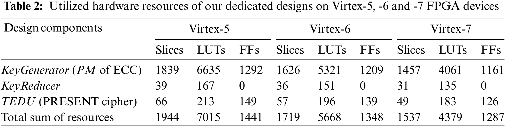
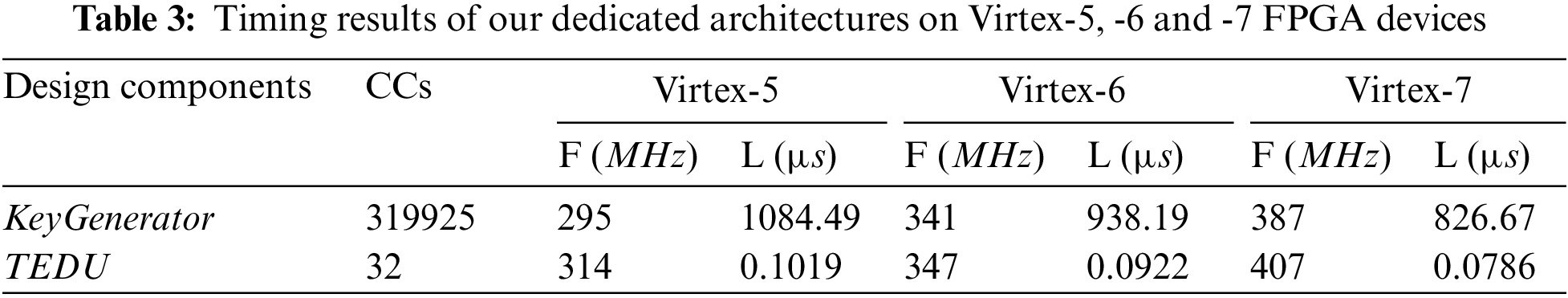
As shown in Table 2, there is a decrease in hardware resource utilization. The reasoning is different implementation technologies. More precisely, the Virtex-5, Virtex-6, and Virtex-7 devices are constructed on 65 nm, 40 nm, and 28 nm process technologies. It is necessary to highlight that these technologies’ names imply the transistor size. For example, the modern 28 nm technology means that the size of one transistor is 28 nm. So, for modern technology, the utilized resources of our dedicated architectures are less when compared to elder technologies. Table 3 demonstrates that the proposed ECC and PRESENT designs result in higher circuit frequencies of 387 MHz and 407 MHz on modern Virtex-7 FPGA devices. As seen in Table 3, the clock cycle required for our KeyGenerator unit is 319925. Table 3 shows that higher cycle counts result in higher latency (i.e., the time required to compute one cryptographic operation) even on modern 28 nm Virtex-7 FPGA. This happens due to a schoolbook multiplier architecture (using shift and add). Amongst several other solutions, one is to use bit-parallel or digit-parallel multipliers to reduce the clock cycle requirement of our dedicated designs. The power values are not reported in tables; however, on the Virtex-5 device, the total power consumption of our KeyGenerator and TEDU units is 16 µW and 8 µW.
4.1.2 Results for Flexible Design
On the same Virtex-5, Virtex-6, and Virtex-7 FPGA devices, our flexible design’s area, timing, and power results are presented in Table 4. The implementation device is shown in column one. Columns two to four provide the area utilization regarding slices, LUTs, and FFs. Moreover, columns five to seven provide the timing information in terms of total clock cycles (CCs), operational frequency (F in MHz), and latency (L in µs). Finally, the last column shows the total power (i.e., static + dynamic) in µW.
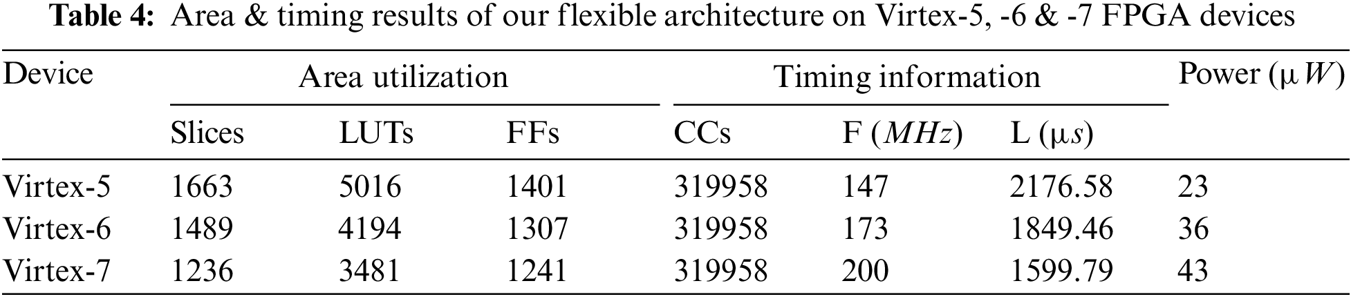
As shown in Table 4, the FPGA slice utilization of our proposed flexible architecture is 1663, 1489, and 1236 on Xilinx Virtex-5, Virtex-6, and Virtex-7 devices. Moreover, the clock cycle requirement of our flexible design is 319958. On different FPGA devices, our flexible design can operate at a maximum of 147 MHz (on Virtex-5), 173 MHz (on Virtex-6), and 200 MHz (on Virtex-7). Similarly, the computation cost of our flexible design for one key generation with encryption/decryption is 2176.58 µs (on Virtex-5), 1849.46 µs (on Virtex-6), and 1599.79 µs (on Virtex-7). As can be observed from Table 4, the proposed architecture outperforms in area, frequency, and latency on a 28 nm Virtex-7 FPGA when compared to Virtex-5 and Virtex-6 implementations. The last column shows that the proposed design consumes less power, i.e., 23 µW, on the Virtex-5 device. As expected, when moving from Virtex-5 to Virtex-7 devices, the increase in circuit frequency increases consumed power.
4.1.3 Comparison of Dedicated and Flexible Designs
Let us compare only the hardware resources of our flexible design with the sum of resources of our dedicated architectures. The flexible design utilizes 1.16 (ratio of 1944 over 1663), 1.15 (ratio of 1719 over 1489), and 1.24 (ratio of 1537 over 1236) times lower slices on Virtex-5, Virtex-6, and Virtex-7 devices. The reason is fewer (design) interfaces for ECC and PRESENT implementations. Moreover, the shared key register between ECC and PRESENT is another cause of obtaining fewer implementation resources. Despite the hardware resources, the consumed power on Virtex-5 of our flexible design is 23 µW, almost equal to the sum of the power of our dedicated implementations of ECC and PRESENT algorithms (16 µW + 8 µW). Almost equal power consumption is due to a schoolbook multiplier in the ECC design, which incorporates only one shift register and an accumulated register. But, in the case of a dedicated PRESENT implementation, the consumed power is 8 µW on Virtex-5 FPGA, while the flexible design consumes 23 µW. This reveals that implementing the PRESENT algorithm in flexible design degrades the performance regarding power consumption, but there is always a trade-off.
4.2 Comparison with State-of-the-Art
Our design implements ECC and PRESENT algorithms and is the first flexible hardware accelerator to our best; therefore, it is essential to highlight that no unified hardware implementation of ECC & PRESENT exists in the literature. Hence, a realistic and reasonable comparison with state-of-the-art is not possible. However, Table 5 compares the most relevant state-of-the-art designs, where column one shows the reference architectures. The key length in n/m is presented in column two, where n shows the key size for symmetric algorithms, and m determines the key length of ECC. The implementation device is listed in column three. Columns four and five provide the area in slices and LUTs for FPGAs, and gate equivalents (GE) show the hardware area for ASIC-implemented designs. Column six presents the clock cycles. Columns seven and eight exhibit the circuit frequency (in MHz) and computation time (i.e., latency in µs), respectively. The last column shows the design details. Moreover, we have used the symbol ‘–’ in Table 5, where the related information is not provided in the reference design.
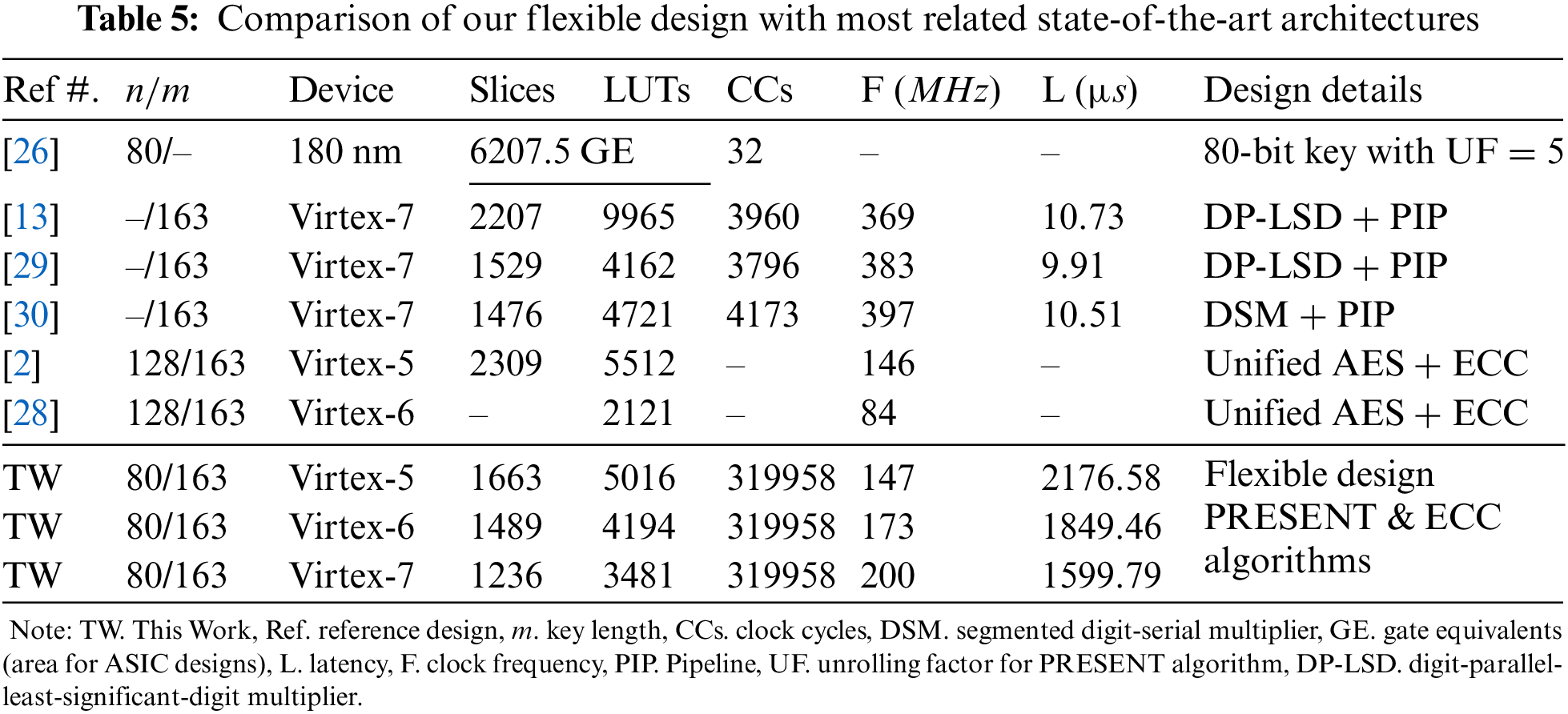
4.2.1 Comparison to PRESENT Algorithm [26]
Column three of Table 5 shows that the implementation results are reported on 180 nm ASIC technology, while we provide results after place-and-route on FPGA. Therefore, on different implementation technologies, the area comparison is not possible. As reported earlier, we implemented the PRESENT architecture of [31] in this work. So, the clock cycle utilization of 32—given in column six of Table 5—is the same for the 80-bit key length variant of a PRESENT cipher. The comparison to frequency and latency is impossible as the corresponding information is not reported in the reference design.
4.2.2 Comparison to PM Designs of ECC [13,29,30]
For an ECC key length of 163 on a Virtex-7 FPGA device, our flexible design is 1.78 (ratio of 2207 over 1236) times more efficient in hardware resources (slices) when compared to the design of [13]. The reason is 8 × 163 register array in [13] while we used only a 5 × 163 register array to keep the initial, intermediate, and final results of PM computation of ECC. Another reason is a digit-parallel-least-significant-digit (DP-LSD) multiplier with a digit size of 32 bits in the datapath of the PM design [13]. On the other hand, we have a shift and add multiplier circuit in the datapath for polynomial squares, multiplication, and inverse computations. Additionally, the design of [13] utilizes a specific square unit for modular square calculations, while we used the resources of our multiplier (of shift and add) to compute square instructions. Along with different multiplier and square units in [13], two reduction units are utilized for modular reduction computations, connected one after multiplier and square unit. In this work, we used only one modular reduction unit as we have only one multiplier. Compared to our flexible architecture, separate modular multiplier and square units in [13] result in lower clock cycles and latency values, reported in columns six and eight of Table 5. A 2-stage pipelining in [13] results in higher operating frequency when compared to our flexible design on the same Virtex-7 FPGA device.
Similar to [13], for the same key length size of 163-bit, our flexible design is 1.23 (ratio of 1529 over 1236) times more efficient in hardware resources (slices) compared to the design of [29]. The reason is the 8 × 163 register array in [29], while we used only a 5 × 163 register array to accommodate ECC’s initial, intermediate, and final results. Another reason is a DP-LSD multiplier in the datapath of the design [29]. We utilized a bit-serial (shift and add) multiplication method for polynomial squares, multiplication, and inverse computations. Compared to our flexible architecture, the DP-LSD multiplier in [29] results in lower clock cycles and latency values, as shown in columns six and eight of Table 5. Alike [13], 2-stage pipelining in [29] results in higher operating frequency when compared to our flexible design on the same Virtex-7 FPGA device.
On identical Virtex-7 FPGA, our flexible architecture is 1.19 (ratio of 1476 over 1236) times more efficient in hardware area (slices) as compared to [30]. The possible reasons to utilize higher hardware resources in [30] are (i) a segmented digit-serial multiplier (DSM) for polynomial multiplications, (ii) separate multiplier and square units for polynomial multiplication and squaring, and (iii) different modular reduction units. In this work, we utilized only one multiplier and one reduction unit. Similar to [29], the PM architecture of [30] is more efficient in clock cycles, circuit frequency, and latency when compared to our flexible design because the designs of [29,30] are pipelined (PIP), while we are not taking pipeline in consideration to this work.
4.2.3 Comparison to Unified Designs of ECC [2,28]
On the Virtex-5 FPGA device, our flexible architecture of PRESENT and ECC algorithms is 1.38 (ratio of 2309 over 1663) times more efficient in slices than the unified design of AES and ECC algorithms of [2]. The AES supports key lengths of 128, 192, and 256; conversely, the PRESENT cipher supports 80 and 128. As we have shown in column two of Table 5 that our PRESENT design utilizes an 80-bit key length while the architecture of [2] targets a 128-bit key length. The larger key lengths infer higher hardware resources. The comparison to clock cycle and latency is impossible as the related information is missing in the reference design. As seen in column seven of Table 5, our flexible architecture operates at a similar circuit frequency of 147 MHz as compared to the frequency reported in [2] (146 MHz). On the Virtex-6 FPGA device, the architecture of [28] is 1.64 (ratio of 3481 over 2121) times more efficient in LUTs than our flexible architecture of PRESENT and ECC algorithms. On the other hand, our flexible architecture is 2.38 (ratio of 200 over 84) times faster in circuit frequency. As seen in columns six and eight of Table 5, the clock cycles and latency comparison is impossible as this information is not present in the reference design.
This article has presented a flexible/unified hardware architecture of ECC and PRESENT algorithms. On Virtex-7 device, our dedicated and flexible designs can operate at a maximum clock frequency of 387 MHz (for ECC), 407 MHz (for PRESENT), and 200 MHz (for flexible). The implementation results of the dedicated and flexible architecture reveal that flexibility directly influences the performance and area of the hardware design. The comparison to state-of-the-art shows that the proposed flexible architecture outperforms hardware resources compared to the unified architecture of ECC and AES [2]. Similarly, our flexible design is faster in clock frequency when compared to a unified implementation of ECC and AES [27]. Consequently, the implementation results and comparison to state-of-the-art show that the proposed architecture is well-suited for applications that demand flexible implementation of cryptographic algorithms.
Funding Statement: The authors would like to thank the Deanship of Scientific Research at Umm Al-Qura University for supporting this work by Grant Code: (22UQU4320020DSR01).
Conflicts of Interest: The authors declare that they have no conflicts of interest to report regarding the present study.
References
1. W. Guo, S. Lian, C. Dong, Z. Chen and X. Huang, “A survey on security of digital microfluidic biochips: Technology, attack, and defense,” ACM Transactions on Design Automation of Electronic Systems (TODAES), vol. 27, no. 4, pp. 1–33, 2022. [Google Scholar]
2. Y. Wang and R. Li, “A unified architecture for supporting operations of aes and ecc,” in 2011 Fourth Int. Symp. on Parallel Architectures, Algorithms and Programming, Tianjin, China, pp. 185–189, 2011. [Google Scholar]
3. M. Rashid, M. Imran, A. R. Jafri and T. F. Al-Somani, “Flexible architectures for cryptographic algorithms: A systematic literature review,” Journal of Circuits, Systems, and Computers, vol. 28, no. 3, pp. 1930003–1–1930003–35, 2019. [Google Scholar]
4. F. Shohaimay and E. S. Ismail, “Improved and provably secure ecc-based two-factor remote authentication scheme with session key agreement,” Mathematics, vol. 11, no. 1, pp. 1–22, 2023. [Google Scholar]
5. P. V. Reddy, A. R. Babu and N. B. Gayathri, “Efficient and secure identity-based strong key-insulated signature scheme without pairings,” Journal of King Saud University—Computer and Information Sciences, vol. 33, no. 10, pp. 1211–1218, 2021. [Google Scholar]
6. W. Wang, H. Xu, M. Alazab, T. R. Gadekallu, Z. Han et al., “Blockchain-based reliable and efficient certificateless signature for IIoT devices,” IEEE Transactions on Industrial Informatics, vol. 18, no. 10, pp. 7059–7067, 2022. [Google Scholar]
7. V. S. Miller, “Use of elliptic curves in cryptography,” In: H. C. Williams (Ed.Advances in Cryptology—CRYPTO ’85 Proceedings, CRYPTO 1985, Lecture Notes in Computer Science, vol. 218, Berlin, Heidelberg: Springer, 1986. [Google Scholar]
8. R. L. Rivest, A. Shamir and L. Adleman, “A method for obtaining digital signatures and public-key cryptosystems,” Communications of the ACM, vol. 21, no. 2, pp. 120–126, 1978. [Google Scholar]
9. L. C. Thungon, N. Ahmed and M. I. Hussain, “Comparison of aes and present block cipher for 6LoWPAN based internet-of-things,” International Journal of Computational Intelligence & IoT, vol. 1, no. 2, pp. 255–259, 2018. [Google Scholar]
10. C. A. Lara-Nino, M. Morales-Sandoval and A. Diaz-Perez, “An evaluation of aes and present ciphers for lightweight cryptography on smartphones,” in Int. Conf. on Electronics, Communications and Computers (CONIELECOMP), Cholula, Mexico, pp. 87–93, 2016. [Google Scholar]
11. D. Hankerson, S. Vanstone and A. Menezes, Guide to elliptic curve cryptography, Springer, pp. 1–311, 2004. [Online]. Available at: https://link.springer.com/book/10.1007/b97644 (last accessed on January 9 2023). [Google Scholar]
12. G. Leelavathi, K. Shaila and K. R. Venugopal, “Hardware performance analysis of rsa cryptosystems on fpga for wireless sensor nodes,” International Journal of Intelligent Networks, vol. 2, pp. 184–194, 2021. [Google Scholar]
13. M. Imran, M. Rashid, A. R. Jafri and M. Kashif, “Throughput/area optimised pipelined architecture for elliptic curve crypto processor,” IET Computers & Digital Techniques, vol. 13, no. 5, pp. 361–368, 2019. [Google Scholar]
14. Z. Liu, X. Huang, Z. Hu, M. K. Khan, H. Seo et al., “On emerging family of elliptic curves to secure internet of things: Ecc comes of age,” IEEE Transactions on Dependable and Secure Computing, vol. 14, no. 3, pp. 237–248, 2017. [Google Scholar]
15. C. A. Lara-Nino, A. Diaz-Perez and M. Morales-Sandoval, “Elliptic curve lightweight cryptography: A survey,” IEEE Access, vol. 6, pp. 72514–72550, 2018. [Google Scholar]
16. W. Diffie and M. Hellman, “New directions in cryptography,” IEEE Transactions on Information Theory, vol. 22, no. 6, pp. 644–654, 1976. [Google Scholar]
17. M. Rashid, S. S. Jamal, S. Z. Khan, A. R. Alharbi, A. Aljaedi et al., “Elliptic-curve crypto processor for rfid applications,” Applied Sciences, vol. 11, no. 15, pp. 7079, 2021. [Google Scholar]
18. Y. -P. Liao and C. -M. Hsiao, “A secure ecc-based rfid authentication scheme integrated with id verifier transfer protocol,” Ad Hoc Networks, vol. 18, pp. 133–146, 2014. [Google Scholar]
19. D. He and S. Zeadally, “An analysis of rfid authentication schemes for internet of things in healthcare environment using elliptic curve cryptography,” IEEE Internet of Things Journal, vol. 2, no. 1, pp. 72–83, 2015. [Google Scholar]
20. M. E. S. Saeed, Q. -Y. Liu, G. Tian, B. Gao and F. Li, “Remote authentication schemes for wireless body area networks based on the internet of things,” IEEE Internet of Things Journal, vol. 5, no. 6, pp. 4926–4944, 2018. [Google Scholar]
21. M. Li, D. Zhao, X. Tang, S. Cheng, X. Hu et al., “Hardware implementation and optimization design of lightweight rectangle algorithm,” in IEEE 9th Joint Int. Information Technology and Artificial Intelligence Conf. (ITAIC), Chongqing, China, pp. 1447–1450, 2020. [Google Scholar]
22. C. T. O. Otero, J. Tse and R. Manohar, “AES hardware-software co-design in wsn,” in 21st IEEE Int. Symp. on Asynchronous Circuits and Systems, Mountain View, CA, USA, pp. 85–92, 2015. [Google Scholar]
23. S. Abed, R. Jaffal, B. J. Mohd and M. Alshayeji, “Fpga modeling and optimization of a simon lightweight block cipher,” Sensors, vol. 19, no. 4, pp. 913, 2019. [Google Scholar] [PubMed]
24. S. Limnaios, N. Sklavos and O. Koufopavlou, “Lightweight efficient simeck32/64 crypto-core designs and implementations, for iot security,” in IFIP/IEEE 27th Int. Conf. on Very Large Scale Integration (VLSI-SoC), Cuzco, Peru, pp. 275–280, 2019. [Google Scholar]
25. W. E. Youssef, A. Abdelli, F. Dridi and M. Machhout, “Hardware implementation of secure lightweight cryptographic designs for IoT applications,” Security and Communication Networks, vol. 2020, pp. 13, 2020. [Google Scholar]
26. B. Rashidi, “Efficient and high-throughput application-specific integrated circuit implementations of hight and present block ciphers,” IET Circuits, Devices & Systems, vol. 13, no. 6, pp. 731–740, 2019. [Google Scholar]
27. S. Nagaraja and V. Sridhar, “A unified architecture for a dual field ecc processor applicable to aes,” in Fifth Int. Conf. on Computational Intelligence, Modelling and Simulation, Seoul, Korea (Southpp. 321–326, 2013. [Google Scholar]
28. L. Parrilla, E. Castillo, J. A. Lopez-Ramos, J. A. Alvarez-Bermejo, A. Garcia et al., “Unified compact ecc-aes co-processor with group-key support for iot devices in wireless sensor networks,” Sensors, vol. 18, no. 1, pp. 251, 2018. [Google Scholar] [PubMed]
29. M. Imran, S. Pagliarini and M. Rashid, “An area aware accelerator for elliptic curve point multiplication,” in 27th IEEE Int. Conf. on Electronics, Circuits and Systems (ICECS), Glasgow, UK, pp. 1–4, 2020. [Google Scholar]
30. Z. -U. -A. Khan and M. Benaissa, “Throughput/area-efficient ecc processor using montgomery point multiplication on fpga,” IEEE Transactions on Circuits and Systems II: Express Briefs, vol. 62, no. 11, pp. 1078–1082, 2015. [Google Scholar]
31. A. Bogdanov, L. R. Knudsen, G. Leander, C. Paar and A. Poschmann, “Present: An ultra-lightweight block cipher,” In: P. Paillier, I. Verbauwhede (Eds.Cryptographic Hardware and Embedded Systems–CHES 2007, Lecture Notes in Computer Science, vol. 4727, Berlin, Heidelberg: Springer, 2007. [Google Scholar]
32. L. Chen, D. Moody, A. Regenscheid and A. Robinson, “Recommendations for discrete logarithm-based cryptography: Elliptic curve domain parameters,” NIST Special Publication (NIST SP 800-186), 2023. [Online]. Available: https://nvlpubs.nist.gov/nistpubs/SpecialPublications/NIST.SP.800-186.pdf (last accessed on April 4, 2023). [Google Scholar]
33. T. Itoh and S. Tsujii, “A fast algorithm for computing multiplicative inverses in gf(2m) using normal bases,” Information and Computation, vol. 78, no. 3, pp. 171–177, 1988. [Google Scholar]
Cite This Article
 Copyright © 2023 The Author(s). Published by Tech Science Press.
This work is licensed under a Creative Commons Attribution 4.0 International License , which permits unrestricted use, distribution, and reproduction in any medium, provided the original work is properly cited.
 Downloads
 Citation Tools