
 Submit a Paper
 Propose a Special lssue
 Open Access
ARTICLE

FPGA Optimized Accelerator of DCNN with Fast Data Readout and Multiplier Sharing Strategy
College of Electronic Science and Technology, National University of Defense Technology, Changsha, 410073, China
* Corresponding Author: Qingjiang Li. Email:
Computers, Materials & Continua 2023, 77(3), 3237-3263. https://doi.org/10.32604/cmc.2023.045948
Received 12 September 2023; Accepted 03 November 2023; Issue published 26 December 2023
 View Full Text
 Download PDF
Abstract
With the continuous development of deep learning, Deep Convolutional Neural Network (DCNN) has attracted wide attention in the industry due to its high accuracy in image classification. Compared with other DCNN hardware deployment platforms, Field Programmable Gate Array (FPGA) has the advantages of being programmable, low power consumption, parallelism, and low cost. However, the enormous amount of calculation of DCNN and the limited logic capacity of FPGA restrict the energy efficiency of the DCNN accelerator. The traditional sequential sliding window method can improve the throughput of the DCNN accelerator by data multiplexing, but this method’s data multiplexing rate is low because it repeatedly reads the data between rows. This paper proposes a fast data readout strategy via the circular sliding window data reading method, it can improve the multiplexing rate of data between rows by optimizing the memory access order of input data. In addition, the multiplication bit width of the DCNN accelerator is much smaller than that of the Digital Signal Processing (DSP) on the FPGA, which means that there will be a waste of resources if a multiplication uses a single DSP. A multiplier sharing strategy is proposed, the multiplier of the accelerator is customized so that a single DSP block can complete multiple groups of 4, 6, and 8-bit signed multiplication in parallel. Finally, based on two strategies of appeal, an FPGA optimized accelerator is proposed. The accelerator is customized by Verilog language and deployed on Xilinx VCU118. When the accelerator recognizes the CIRFAR-10 dataset, its energy efficiency is 39.98 GOPS/W, which provides 1.73 × speedup energy efficiency over previous DCNN FPGA accelerators. When the accelerator recognizes the IMAGENET dataset, its energy efficiency is 41.12 GOPS/W, which shows 1.28 × −3.14 × energy efficiency compared with others.Keywords
In recent years, with the rapid development of artificial intelligence, various applications based on DCNN have attracted extensive attention in the industry. DCNN has not only made meaningful progress in the field of computer vision, such as image recognition and detection [1], target tracking [2], and video surveillance [3], but also made breakthroughs in other areas, such as natural language processing [4] network security [5], big data classification [6], speech recognition [7], and intelligent control [8].
Currently, the mainstream hardware deployment platforms of DCNN include CPU, ASIC, FPGA, etc. The advantages of CPU are mature micro-architecture and advanced semiconductor device technology, but its serial computing mechanism limits the operational speed of DCNN. ASIC is integrated circuits designed and manufactured according to user demand. It has the advantages of high computing speed and low energy consumption, but its disadvantages are high design cost and time cost. FPGA is a field programmable gate array, allowing repeated programming, and has the advantages of low energy consumption, parallelism, and low cost, so FPGA can be used in parallel computing, cloud computing [9], neural network inference [10,11], and other aspects.
However, the enormous network parameters and computing scale of DCNN, as well as the limited logic capacity of FPGA, make hardware deployment on FPGAs inefficient. In order to improve the operation speed, various methods including data multiplexing [12], network quantization [13–15], and network pruning [16,17] are proposed. The traditional sequential sliding window (SSW) method [18,19] has two drawbacks. One is that the multiplexing rate between rows of sliding window data is low, and the other one is that the storage order of the operation results is not convenient for the operation of the pooling layer. Besides, much previous research into reducing the energy consumption of FPGA mainly focused on the improvement of the utilization of FPGA resources. DCNN has numerous multiplications, which will occupy many DSP blocks on the FPGA. DSP48E2 on Xilinx FPGA supports 27 bit × 18 bit multiplication. After network quantization, the data width of multiplication is often 8 bits or less, so multiple multiplications can be completed on a single DSP [20] The SIMD architecture proposed in [21] supports the multiplication of two groups of 8-bit data by a single DSP. The disadvantage is that the input data of two groups of multiplication are the same, and the input data are unsigned numbers. The SDMM architecture proposed in [22] supports six groups of 4-bit data multiplication, four groups of 6-bit data multiplication, or three groups of 8-bit data multiplication on a single DSP. However, its disadvantage is that the quantified weight needs to be further processed, which will make the weight deviate from the actual value, for example, 5-bit weight data is 10011, but the actual weight data used for calculation is 10010, thus affecting the accuracy of the quantification network. In addition, the operation needs to be supplemented by shift registers and adders for calculation, which will increase the overhead of other logical resources. In recent years, Xilinx’s official white paper has proposed a structure [23] to achieve a single DSP (DSP48E2) to achieve four groups of 4-bit data multiplication. But the structure requires that the input data is unsigned data, the input data of each two groups of multiplication is the same, and the weight data of each two groups of multiplication is the same.
In order to improve the energy efficiency of DCNN deployed on FPGA, this paper proposed an FPGA optimized accelerator, which focuses on improving the operation speed and reducing energy consumption. 1) A circular sliding window (CSW) data reading method is proposed, compared with other methods, the ‘down-right-up-right’ circular sliding window mechanism is adopted to read the input data. Some input data between rows are multiplexed via this method, so the CSW data reading method can take less time to finish the data reading of a single channel. What’s more, the CSW data reading method lets output data in adjacent locations, which can save the data rearrangement time consumption before entering the pooling unit. 2) Two types of customized multipliers are introduced to implement multi-groups of signed data multiplication in a single DSP, compared with other multipliers, the customized multipliers in this paper use sign-magnitude representation to encode signed data, so, without bit expansion or result correcting. The customized multipliers in this paper can still support the operation that both weight data and input data are signed data.
2 Energy Efficiency Improvement Strategies
This chapter mainly introduces two strategies of the FPGA optimized accelerator to improve energy efficiency. Firstly, the operation speed of FPGA based DCNN accelerator is improved through the fast data readout strategy. Secondly, the multiplier sharing strategy is adopted to reduce the energy consumption of FPGA.
2.1 Fast Data Readout Strategy
In order to improve the operation speed of the FPGA-based DCNN accelerator, the research can be carried out from two aspects: reducing the data bandwidth requirement during network operation and reducing the amount of network computation. This paper mainly studies from the perspective of reducing the data bandwidth requirements during network operations.
There are numerous multiplication and accumulation operations in the operation process of DCNN, but limited by the logical capacity of FPGA, DCNN often only performs single-layer partial multiplication and addition operations, so it is necessary to store the intermediate data generated by the operation. Considering that the memory bandwidth of FPGA is fixed, it is necessary to reduce the data bandwidth requirement of network operation. There are three main methods to reduce the data bandwidth requirement of network operation: data multiplexing, network quantification, and standardized data access patterns. This paper mainly uses data multiplexing and network quantification.
Data multiplexing achieves the purpose of acceleration by reducing the access frequency to memory, which is generally divided into three types [12]: input multiplexing, output multiplexing, and weight multiplexing. Input multiplexing generally refers to multiplexing the data in the input buffer, thereby reducing the access frequency of the input buffer to the on-chip memory. Weight multiplexing generally refers to reducing the frequency of accesses to off-chip memory. The weights are generally stored in off-chip memory. Output multiplexing generally refers to multiplexing the data in the output register, thereby reducing the memory access frequency of the intermediate data. The FPGA optimized accelerator proposed in this paper uses these three data multiplexing methods. For input multiplexing, a fast data readout strategy is proposed, it can further improve the multiplexing rate of input data via a CSW data reading method.
As shown in Fig. 1, the traditional SSW data reading method uses the ‘always right’ sequential sliding window mechanism to read the input data. The CSW data reading method proposed in this paper uses the ‘down-right-up-right’ circular sliding window mechanism to read the input data. Both these two methods can be applied to process multiple channels in parallel. There are two advantages of the proposed CSW data reading method.

Figure 1: The CSW data reading method and the traditional SSW data reading method
The first advantage, as shown in Fig. 2, is that for each input channel, the time cost of the CSW data reading method is less than that of the SSW data reading method. When kernel size is 3, and stride length is 1, the SSW data reading method spends 18 clock cycles reading the first 4-group input data of each row. Compared with the SSW data reading method, the CSW data reading method only spends 16 clock cycles reading the first 4-group input data of each row. Because in the ‘r4’ state, the SSW data reading method needs to read 3 new input data, but the CSW data reading method only 1 new input data. In addition, the SSW data reading method spends 12 clock cycles reading the non-first 4-group input data of each row. Compared with the traditional SSW data reading method, the CSW data reading method only spends 8 clock cycles reading the non-first 4-group input data of each row. Because in the ‘r2’ and ‘r4’ states, the SSW data reading method needs to read 3 new input data, but the CSW data reading method only reads 1 new input data.

Figure 2: Time cost of the CSW and SSW data reading method
The proposed method could be extended to neural networks with different sizes of kernel, padding, and stride. If the size of the input channel is N, the number of padding is P, the stride is S, kernel size is K, to read each channel of one convolutional layer in parallel, the time cost of SSW and CSW data reading method is shown in Eqs. (1) and (2), respectively. SSW data reading method utilizes K rows of input data to obtain 1 row of output data. Compared with the traditional SSW data reading method, the CSW data reading method fully utilizes S + K rows of input data to efficiently obtain 2 rows of output data.
The saving ratio of time cost defined by (T1−T2)/T1 is shown in Eq. (4), and Fig. 3 illustrates the saving ratio of time cost of frequently-used strides (1, 2) and kernel size (3 × 3, 5 × 5, 7 × 7). Commonly, kernel size is larger than stride length in neural networks, such as Resnet50, MobileNetV3, YoloV3, etc. When the stride is the same, the saving ratio has a positive correlation with kernel size. When the kernel size is the same, the saving ratio has a negative correlation with stride. It can be also found that the saving ratio is irrelevant to padding size P and input channel size S.

Figure 3: Saving ratio of clock cycles of various strides and kernel size
The second advantage, as shown in Fig. 4 is that for the pooling layer, the cache space of the CSW data reading method is less than that of the SSW data reading method. When both kernel size and stride in the pooling layer are 2, the SSW data reading data method cannot directly produce 4 output data in adjacent locations, the pooling operation only starts until obtaining one row of output data, which needs additional cache space to save other output data. Compared with the traditional SSW data reading method, the CSW data reading method can produce every 4 output data in adjacent locations, then the pooling operation can be completed directly, which doesn’t need cache space to save other output data.
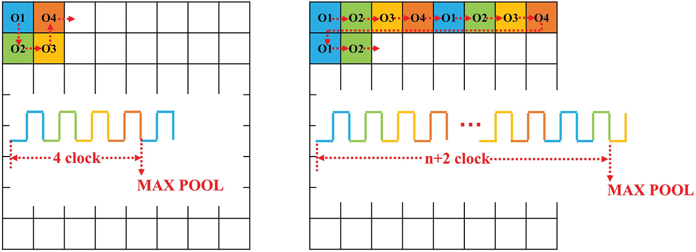
Figure 4: The output data position of the CSW method (left) and the SSW method (right)
The stride length and kernel size of the pooling layer could affect the size of the cache space. Table 1 summarizes the number of output data rows needed to be cached. When both kernel size and stride length are even or odd, such as MobileNet, and VGG, which have the same size of stride and kernel size in the pooling layer, the CSW data reading method requires less cache space to save other data than SSW data reading method.

The fast data readout strategy mainly improves the speed of input data reading, so it is applied to the INPUT CU unit of the FPGA optimized accelerator.
2.2 Multiplier Sharing Strategy
In order to reduce the energy consumption of FPGA, this paper mainly studies from the perspective of reducing the resource consumption of FPGA. Because the core operations of the convolutional layer and the fully connected layer are both multiplication and addition operations, this paper uses the method of multiplexing the same operation array with the full connection layer and the convolution layer to improve the resource utilization of FPGA. In addition, since DCNN is quantized, the data width of multiplication is 8 bits or less. One DSP on FPGA supports a group of 27 bit × 18 bit multiplications. Therefore, a multiplier sharing strategy could be applied. The multiplier in the operation array is customized, where each DSP can simultaneously complete two or three groups of multiplication to reduce the resource consumption of FPGA.
In this paper, sign-magnitude representation is used to encode signed data. For example, −4 is expressed as 1_00100, and 4 is expressed as 0_00100. The ordinary DSP block of an off-the-shelf FPGA device is modified to a Signed-Signed Three Multiplication (SSTM) unit or a Signed-Signed Double Multiplication (SSDM) unit. The SSTM architecture supports one DSP to complete the multiplication of three groups of 6-bit signed data at the same time, but the three groups of multiplication need to maintain the same input data or weight data. The SSDM architecture supports one DSP to complete two groups of 6-bit signed data multiplication at the same time. The input data and weight data of the two groups of multiplication can be different. The sign bit and magnitude bits in the proposed two structures are operated separately. The sign bit is operated by XOR gates, and the magnitude bit is operated by ordinary DSP. This paper mainly introduces the structure of SSTM and SSDM when the data width is 6, but SSTM and SSDM can also apply to other data widths.
As shown in Fig. 5, the structure of the PE3 unit, an operation unit of the operation array, consists of four SSTM units. A single SSTM unit adopts the structure of a multiplier with three groups of multiplications completed by one DSP at the same time.

Figure 5: PE3 unit architecture
The sign bits of the input data (in [5]) and the sign bits of the three groups of weight data (w1[5], w2[5], w3[5]) are extracted for XOR operation, respectively. The sign bits of three groups of multiplication output data can be obtained.
Fig. 6 shows the magnitude bits operation mode of SSTM. Firstly, the magnitude bits of the weight data of three groups of multiplication are extracted. Then, a new 25-bit weight data is formed by inserting 5-bit 0 data between the magnitude bits of the three groups of weight data. Finally, the 25-bit weight data and the magnitude bits of the input data are multiplied to obtain 30-bit output data. The high 10 bits, middle 10 bits, and low 10 bits of the extracted 30-bit output data are the magnitude bits of the output data of the first group, the second group, and the third group of multiplication.

Figure 6: Magnitude bits operation mode of SSTM
Considering the number of convolutional kernels in the networks is always an integer multiple of 4. If the accelerator only uses the SSTM structure, it will result in some DSPs not working during the calculation of each convolutional layer not work, which will reduce DSP efficiency, so the accelerator also adopts some SSDM structures that can support input data be different.
As shown in Fig. 7, the structure of the PE2 unit, an operation unit of the operation array, consists of two SSDM units. A single SSDM unit adopts the structure of a multiplier with two groups of multiplications completed by one DSP at the same time.

Figure 7: PE2 unit architecture
The two groups’ sign bits of the input data (in1[5], in2[5]) and the sign bits of the two groups of weight data (w1[5], w2[5], w3[5]) are extracted for XOR operation, respectively. The sign bits of two groups of multiplication output data can be obtained.
Fig. 8 shows the magnitude bits operation mode of SSDM. Firstly, the magnitude bits of the weight data of two groups of multiplication operations are extracted, and the magnitude bits of the input data of two groups of multiplication are extracted. Then, a new 25-bit weight data is formed by inserting 15-bit 0 data between the magnitude bits of the three groups of weight data, and a new 15-bit input data is formed by inserting 5-bit 0 data between the magnitude bits of the three groups of weight data. Finally, the 25-bit weight data and the 15-bit input data are multiplied to obtain 40-bit output data. The high 10 bits and low 10 bits of the extracted output data are the magnitude bits of the output data of the first group and the second group of multiplication.
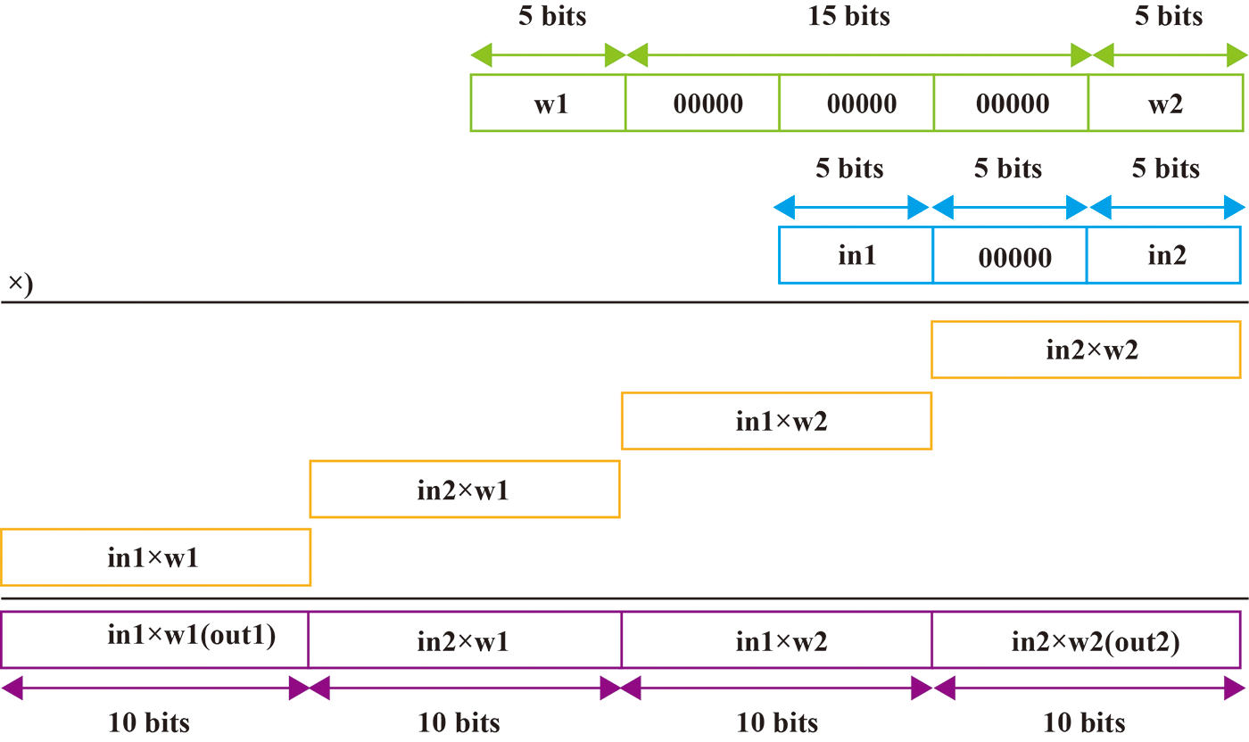
Figure 8: Magnitude bits operation mode of SSDM
Besides, SSTM and SSDM structures can also apply to data whose data width is not 6. As shown in Table 2, it gives how many multiplications can be implemented by SSTM structure when data width is 4, 6, 8, the smaller the data width, the more multiplication can be implemented by SSTM structure. As for the SSDM structure, for various data widths, it can only implement 2 groups of multiplication, and the largest data is 6, which is limited by the data width of DSP48E2. Table 3 gives the data width of new component input data and weight data when the data width of input data and weight data is 4, 5, 6.


Overall, SSTM and SSDM structure can be used in other networks that are quantified, SSDM is limited by quantization precision, while with the development of lightweight networks, more complicated networks can be quantified to lower data width, [24] can quantify the data width of Resnet18 to 4-bit. The multiplier sharing strategy mainly reduces the DSP resource waste of the multiplier, so it is applied to the calculation unit of the FPGA optimized accelerator.
This chapter mainly introduces the hardware circuit structure of the FPGA optimized accelerator. As shown in Fig. 9, the accelerator is mainly divided into three parts: a memory cell, a control unit, and a calculation unit. The memory cell mainly completes the storage of data required for operation, intermediate data for operation, and operating results. The control unit mainly controls the data flow direction of the entire architecture and completes simple operations such as addition, quantization, activation, and pooling. The calculation unit mainly completes the multiplication of the whole network.

Figure 9: Architecture of the FPGA optimized accelerator
The data path of the accelerator is shown in Fig. 9, which is mainly divided into four steps. Firstly, the top control unit (TOP CU) provides control signals to decide the data flow direction of the whole accelerator. Secondly, the input control unit (INPUT CU) reads the input data saved in the RAM group through the RAM selection unit (RAM SEL), at the same time, the weight control unit (WEIGHT CU) reads the weight data saved in FIFO, and both input data and weight data are sent to the PE array. Thirdly, the PE array completes the multiplication of input data and weight data, and the results of the multiplication are sent to the output control unit (OUTPUT CU). Finally, OUTPUT CU reads multiplication results and bias data saved in ROM to complete accumulation, activation, quantification, and max pool calculation, FIFO is used for memory access of intermediate data, and the final results are sent to the RAM group through RAM SEL.
When the parameters of DCNN are quantized, the bit widths of the input data and weight data of each layer of DCNN are the same. Therefore, the proposed architecture only completes the design of the DCNN one-layer circuit structure and then continuously multiplexes the entire circuit until all layers of DCNN are calculated.
The memory cell consists of three parts: DDR4, RAM group, and ROM. DDR4 mainly stores weight data. Because the amount of DCNN weight data is large, on-chip storage resources cannot meet its needs. In addition, considering that the DDR4 read and write clock is inconsistent with the accelerator master clock, it is necessary to add a FIFO unit between the DDR4 and the control unit for buffering. The RAM group mainly stores the transformable data of the DCNN operation process. It is used to store the input data and output data of the DCNN single layer. It is divided into two groups, with 64 RAMs in each group. Since the architecture proposed in this paper is in the form of layer-by-layer calculation, when one group of RAM groups is used as input to provide input data for the control unit, the other group of RAM groups is used as output to save the output data. ROM mainly stores the invariant data during DCNN operation, which is used to store the bias value and quantization parameters of DCNN.
The control unit consists of six parts: TOP CU, INPUT CU, RAM SEL, WEIGHT CU, bias data and quantization parameter control unit (B_Q CU) and OUTPUT CU.
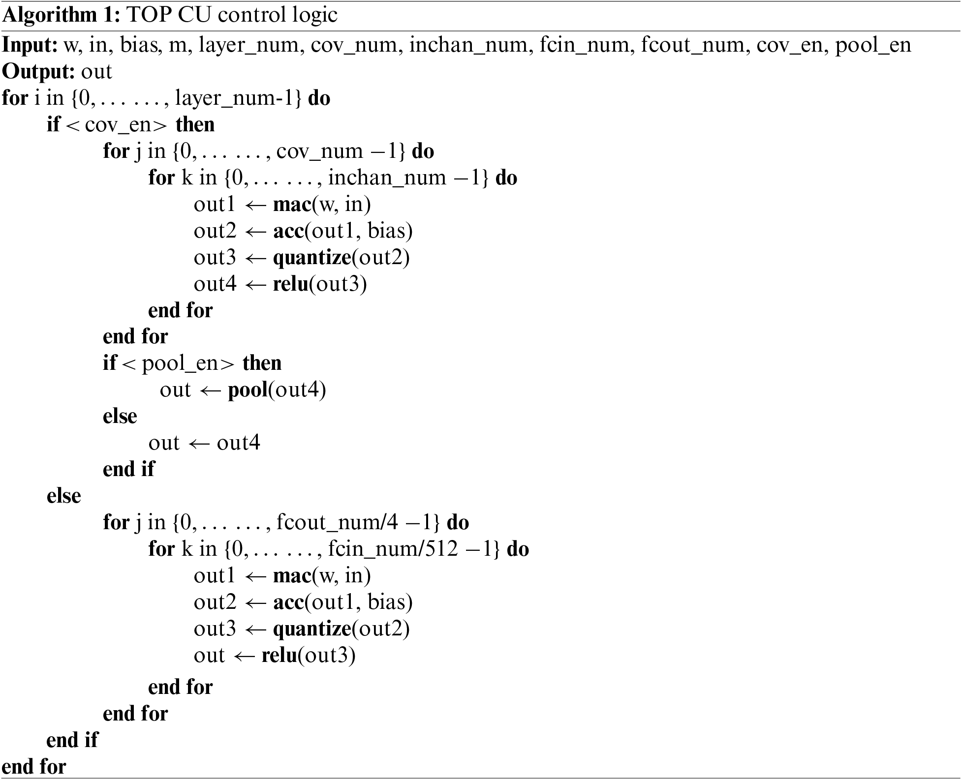
TOP CU unit mainly controls the data flow direction of the entire accelerator and provides hyper-parameters for other control units. Its control logic is shown in Algorithm 1. Since the operation unit can only calculate the multiplication and accumulation of 64 groups of input channels and 4 groups of convolution kernels in parallel, the whole control logic is divided into three cycles. The first loop is expanded to complete the operation of all input channels corresponding to the four groups of convolution kernels in the convolution layer or the operation of 512 input neurons corresponding to 4 output neurons in the fully connected layer. The operation process includes multiplication, quantification, and activation. The second loop is expanded to complete the operation of all convolution kernels in the single-layer convolution layer or the operation of all output neurons in the single-layer fully connected layer. The third loop is expanded to complete the operation of all layers of DCNN, and the corresponding pooling operation is completed according to the number of layers.
INPUT CU unit mainly reads the input data from the memory cell to the calculation unit. As shown in Fig. 10, the INPUT CU unit can read 64 channels of data in parallel and transmit 5 data of each channel to the calculation unit in a single clock cycle. INPUT CU reads the input data using the CSW data reading method.

Figure 10: Input data flow direction
The CSW data reading method contains four states, each state updates 9 input data stored in registers, and 9 input data are transmitted to the calculation unit in 2 cycles. In the first state, the input data in ‘1’, ‘4’, ‘5’, ‘6’ and ‘0’ positions are sent to PE array in the first clock cycle, the input data in ‘2’, ‘6’, ‘9’, ‘6’ and ‘0’ positions are sent to PE array in the second clock cycle, and then, entering the second state through ‘down’ sliding window. In the second state, the input data in ‘5’, ‘8’, ‘9’, ‘12’, and ‘4’ positions are sent to the PE array in the first clock cycle, the input data in ‘6’, ‘10’, ‘13’, ‘14’ and ‘4’ positions are sent to PE array in the second clock cycle, and then, entering the third state through ‘right’ sliding window. In the third state, the input data in ‘6’, ‘9’, ‘10’, ‘13’ and ‘5’ positions are sent to PE array in the first clock cycle, the input data in ‘7’, ‘11’, ‘14’, ‘15’ and ‘5’ positions are sent to PE array in the second clock cycle, and then, entering the fourth state through ‘up’ sliding window. In the fourth state, the input data in ‘2’, ‘5’, ‘6’, ‘9’ and ‘1’ positions are sent to PE array in the first clock cycle, the input data in ‘3’, ‘7’, ‘10’, ‘11’ and ‘1’ positions are sent to PE array in the second clock cycle, and then, entering the first state through ‘right’ sliding window.
The CSW method will make the address of input data control logic more complicated. However, the structure reads 64 input data in the same position of different channels, so if the address of one input channel control logic is implemented, other channels only use the same address. As a result, it has a slight increase in logic resources because of more complicated control logic and has a small effect on the performance of the entire structure.
The OUTPUT CU unit mainly processes the output data of the calculation unit and saves it to the storage unit. As shown in Fig. 11, the OUTPUT CU unit is mainly composed of four COV_FC_OUT units and one COV_ONLY_OUT unit. The COV_FC_OUT unit is composed of 256 input addition trees, accumulators, Q/A units, pooling units, and several multi-channel selectors. It mainly completes the summation of the multiplication results of a row in the first four rows of the PE array and the accumulation of the multiplication and addition results with the first row, as well as the quantification, activation, and pooling operations of the results. In addition, if the PE array cannot calculate all channels at a time, the intermediate data can be temporarily stored in the FIFO unit. The COV_ONLY_OUT unit is composed of a 64-input addition tree, accumulator, SOFTMAX unit, and several multi-channel selectors. It mainly completes the summation of the multiplication results of the third row of the PE array, the accumulation of the bias value, and the accumulation of the calculation results of several channels. When the operation is in the full connection layer, the third row of the operation unit of the PE array is not working, so the 64-input addition tree is also not working. The SOFTMAX unit mainly completes the label value acquisition of the final operation result.
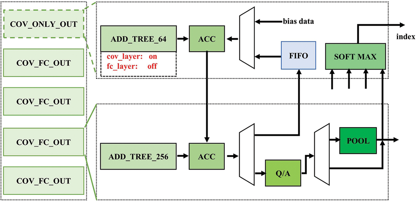
Figure 11: Output data control unit
For the Q/A unit, the quantization and activation operations of the accumulated results are completed. Considering that the quantization parameters are floating-point, in order to avoid the multiplication of floating-point, in this paper, the quantization and activation function is fused. The fusion principle is: The data width of the input data is x-bit, the data width of the output data is 5-bit, and the value range is [0, 31]. As shown in Eq. (7), quantization and activation operations can be regarded as a piecewise function. d1-d31 are piecewise parameters; a is input, and b is output.
As shown in Fig. 12a, the actual hardware deployment uses a 32-channel selector to realize the two operation processes of quantization and activation function. After evaluation, the method that uses a 32-channel selector will cost 306 LUTs and 6 FFs, while the method that uses a float multiplication will cost 329 LUTs and 5 FFs directly. The method used in this work consumes less logic resources. In addition, if M is smaller, more LUTs and FFs will be consumed to prove the accuracy of the calculation.

Figure 12: Q/A unit (a), pooling unit (b) and SOFTMAX unit (c)
For the pooling unit, the accelerator uses the max pooling operation. Considering that the four groups of data of the pooling operation come in different clock cycles, a comparator is used to complete four comparisons in four clocks. For every four comparisons, the non-input end of the comparator is set to 0. The structure is shown in Fig. 12b.
For the SOFTMAX unit, as shown in Fig. 12c, it is composed of four comparators. SOFTMAX is only working in the last layer, which is divided into three clock cycles to complete the maximum value of four output results. The first clock cycle and the second clock cycle obtain the maximum value and label value of the four groups of data. The third clock cycle obtains the maximum value and label of the current four groups of data and the previous four groups of data. Since the output of the last layer is more than four, the maximum value and the label value of the current four groups of data must be saved.
The RAM SEL unit provides input data for the INPUT CU unit to select the corresponding RAM according to the number of layers. The RAM SEL unit selects the corresponding RAM for the OUTPUT CU unit to save the single-layer operation results. WEIGHT CU unit reads the weight data from DDR4 to the FIFO unit and then transmits the weight in the FIFO to the calculation unit. Since the read-and-write clock frequency of DDR4 is faster than the clock frequency of the accelerator, the PING-PONG mechanism is used to read the weight data. B_Q CU unit reads the bias data and quantization parameters required for the operation from the ROM to the OUTPUT CU unit.
The calculation unit is the core unit of the accelerator, completing the multiplication of the convolutional layer and the fully connected layer. As shown in Fig. 13, the calculation unit is a PE array, which is divided into three rows, including 64 PE3 units in the first row, 64 PE2 units in the second row, and 32 PE2 units in the third row. The PE3 unit consists of 4 groups of SSTM, PE2 unit consists of 2 groups of SSDM.
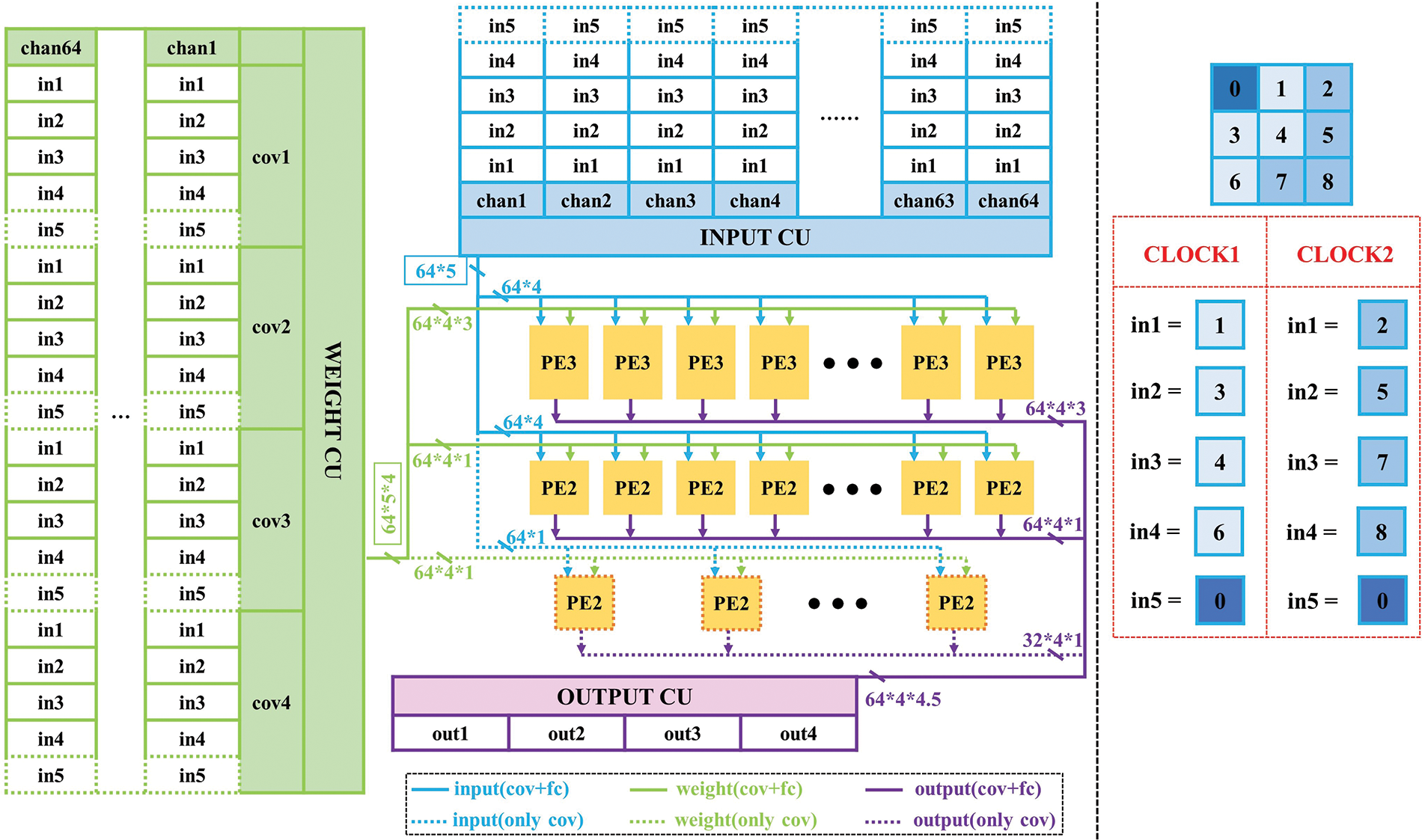
Figure 13: PE array
The input data of the same column in the first row and the second row is the same, and the weight data of each operation unit is different. In addition, the PE array supports two working modes, which are used for the operation of the convolution layer and the fully connected layer, respectively.
In the working mode of the convolution layer: 64 PE3 units and 96 PE2 units are all in a working state, the PE array can complete the multiplication of 64 input channels and 4 convolutional kernels in 2 clock cycles. Because each convolutional kernel has 9 groups of weight data, a single clock cycle of the PE array can complete 1152 (64 × 4 × 9 ÷ 2) groups of multiplication in parallel. The data path is shown in Fig. 13. In the first clock cycle, the corresponding data for ‘1’, ‘3’, ‘4’, and ‘6’ positions are processed by 64 PE3 units and 64 PE2 units. In the second clock cycle, the corresponding data for ‘2’, ‘5’, ‘7’, and ‘8’ positions are processed by 64 PE3 units and 64 PE2 units. 64 PE3 units respond to the multiplication of three groups of convolutional kernels, and 64 PE2 units respond to the multiplication of one group of convolutional kernels. The remaining 32 PE2 units respond to the multiplication of four groups of convolutional kernels in the ‘0’ position.
In the working mode of the fully connected layer: 64 PE3 units in the first row and 64 PE2 units in the second row are in a working state, but 32 PE2 units in the third row are not working. The PE array can complete the multiplication of 512 input neurons and 4 output neurons in 2 clock cycles. A single clock cycle of the PE array can complete 1024 (512 × 4 ÷ 2) groups of multiplication in parallel.
This chapter compares and summarizes the performance parameters of the FPGA optimized accelerator architecture with other published work. Firstly, the network structure used to evaluate and how to complete network quantization is introduced. Secondly, the speed improvement brought by the fast data readout strategy is analyzed and summarized. Thirdly, the energy saving of the multiplier sharing strategy is analyzed. Finally, the overall energy efficiency of the accelerator is evaluated.
4.1 Network Structure and Quantization Result
The datasets should be publicly available to ensure the experiments are reproducible, so the IMAGENET dataset and CIRFAR-10 dataset are selected to be identified by the FPGA optimized accelerator. In addition, as can be seen from Eq. (3), the absolute saving inference delay (Tabsolute) by the fast data readout strategy can also be affected by the image size, so the datasets of two different sizes can be further used to verify the relationship between Tabsolute and image size, the corresponding result will show in Section 4.2. VGG16 [25] is one of the commonly used network structures of DCNN. It covers almost the most basic operations of DCNN, such as multiplication and accumulation operation, batch normalization operation, pooling operation, etc., which makes the experiment have wider applicability. In addition, many previous FPGA accelerators select VGG16 as a DCNN model for testing, which is convenient for the performance evaluation of the accelerator proposed in this paper. Therefore, VGG16 is selected to be a testing DCNN model of the optimized FPGA accelerator.
VGG16 is composed of thirteen convolutional layers and three fully connected layers. After each convolutional layer, it will undergo the bn (batch normalization) layer and activation function. The 13 convolutional layers are divided into five groups. After each group of convolutional layers, a pooling operation is performed to reduce the feature image size. For the CIRFAR-10 dataset, the image size is 32 × 32 × 3. For the IMAGENET dataset [26], the image size is 224 × 224 × 3. The corresponding network structure is shown in Table 4.

According to whether the quantized network needs retraining, the quantization method is divided into PTQ [27,28] (Post-Training Quantization) and QAT [29,30] (Quantization-Aware Training). This paper mainly uses PTQ to quantify the network. The algorithm can convert the parameters of the network from floating points to integers without retraining and has a low impact on the accuracy.
As shown in Fig. 14, the quantization process of a single convolutional layer is shown, and there are three steps. First, the parameters w (weight) and b (bias) of the convolution layer are extracted and fused with the parameters such as μy (mean) and δy2 (variance) of the bn (batch normalization) layer to obtain the corrected parameters w’ (corrected weight) and b’ (corrected bias). The bn layer has been integrated into the weights, so there is no need to deploy the bn layer on the FPGA. Second, the parameters x (input data), w’, and b’ are quantified, respectively. The quantization equations are shown in Eqs. (8)–(10). Third, the quantized input data (qx − Zx), bias data (qb’ − Zb’), and weight data (qw’ − Zw’) are all integers. The quantized input data, bias data, and weight data are used for convolution operation. The result (P) multiplied by the quantization parameter (M, M is floating-point data) and rounded is consistent with the value of the output data after quantization.

Figure 14: The operation flow of PTQ
Using the PTQ algorithm, the accuracy of VGG16 in recognizing CIRFAR-10 under different data widths is obtained, as shown in Fig. 15. It can be seen that the data width is above 5 bits, and the accuracy is reduced by less than 1%. Therefore, this paper selects a network with data width quantized to 5-bit for deployment on FPGA. However, PTQ has the problem of zero offsets. The value range of conventional 5-bit data is [−16, 15]. But the range of 5-bit data obtained by the PTQ algorithm may be [−17, 14], [−13, 18], and so on. Therefore, when the network is deployed on FPGA, it uses a 6-bit width to store 5-bit data.
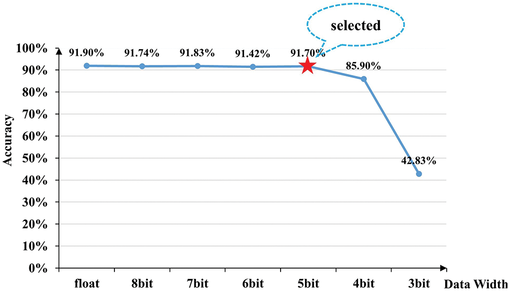
Figure 15: Accuracy under different data widths
4.2 Performance Optimized by Fast Data Readout Strategy
When the accelerator recognizes the CIRFAR-10 dataset, the system clock frequency of the accelerator is 200 MHz, and the latency for inferring one image is 2.02 ms, so the throughput of the accelerator can be calculated, which is 310.62GOPS. When the accelerator recognizes the IMAGENET dataset, the system clock frequency of the accelerator is 150 MHz, and the latency for inferring one image is 98.77 ms, the corresponding throughput is 313.35GOPS.
Fig. 16 illustrates the latency of all convolutional layers when using the CSW data reading method and SSW data reading method during network inference, the inference-saving delay of each layer by the CSW data reading method can be seen. For the CIRFAR-10 dataset, as shown in Fig. 16a, the convolutional layer latency of the CSW data reading method is 0.667 × −0.724× that of the SSW data reading method. Similarly, for the IMAGENET dataset, as shown in Fig. 16b, the convolutional layer latency of the CSW data reading method is 0.667 × −0.669× that of the SSW data reading method. It can be observed that the relative time savings vary across different layers. This is because the accelerator cannot complete all the multiplication and accumulation operations within a single layer. When switching convolution kernels or input channels, there is a clock switching time of 2–3 cycles. The impact of clock switching is greater for smaller input image sizes. For example, in the CIRFAR-10 dataset, the input image sizes of layers 11–13 are 2 × 2, resulting in a relative time savings of approximately 0.276. In contrast, all input layers in the IMAGENET dataset have image sizes of 14 × 14 or larger, leading to a relative time savings of approximately 0.33× for all layers.

Figure 16: Two methods to infer the delay of each layer of one image: (a) IMAGENET (b) CIRFAR-10
Table 5 shows the saved inference time in each convolutional layer using the CSW data reading method, the relation between image size and saving delay by the CSW data reading method can be found. The accelerator’s calculation unit utilized 4 convolution kernels and 64 channels for convolutional operations. Hence, based on the number of input channels and convolution kernels in Table 4, we can obtain the calculation rounds represented by the “epoch” column in Table 5 for each convolutional layer. Then, using these calculation rounds, we can determine the delay savings of individual channels represented by the “delay/image” column in Table 5. From the data in the table, it can be observed that the delay savings of individual channels are positively correlated with the image size. Although the time saved for inference in a single channel from layers 11 to 13 of the IMAGNET dataset is higher than the time saved in a single channel from layers 3 to 4 of the CIFAR-10 dataset, the input image size for layers 11 to 13 of the IMAGNET dataset is smaller than the input image size for layers 3 to 4 of the CIFAR-10 dataset. This difference is caused by the fact that the system clock of the accelerator is lower when processing the IMAGNET dataset compared to when processing the CIFAR-10 dataset. Therefore, the time saved for inference in a single channel is inversely correlated with the system clock of the accelerator.

4.3 Performance Optimized by Multiplier Sharing Strategy
Table 6 shows the resource consumption of the accelerator when recognizing the CIFAR-10 dataset, while Table 7 shows the resource consumption when recognizing the IMAGENET dataset, the difference in various types of hardware resource consumption when the accelerator recognizes the different sizes of the dataset can be concluded, and DSP consumption can be used to evaluate the DSP efficiency of the accelerator. For the recognition tasks of these two datasets, there is no significant difference in logic resource consumption, but the focus is on storage resource consumption. It is worth noting that due to the larger intermediate image size of the IMAGENET dataset, more BRAM resources are required for storing the intermediate image data. This is a unique characteristic of the FPGA optimized accelerator. For deeper convolutional neural networks, there will not be a significant increase in logical resource usage, and the increase in storage resources will only manifest when the intermediate image size grows larger.


The energy consumption of various hardware resources when deploying the accelerator on an FPGA is shown in Fig. 17, the energy influence of different hardware resources can be found, and energy consumption can be used to evaluate the energy efficiency of the accelerator. It is worth noting that the IMAGENET dataset has lower energy consumption for DSP and LOGIC resources compared to the CIFAR-10 dataset. However, the logical resource overhead is similar for both datasets. This energy consumption difference is due to the different system clocks used for the two datasets, as using a lower system clock reduces energy consumption. According to the experimental data in Tables 6 and 7, the BRAM resource overhead required for the IMAGENET dataset is 11.36 × higher compared to the CIFAR-10 dataset. However, it is worth noting that the IMAGENET dataset only consumes an additional 1.227 W of energy compared to the CIFAR-10 dataset in terms of BRAM power consumption. This indicates that the energy cost overhead of BRAM is relatively low.
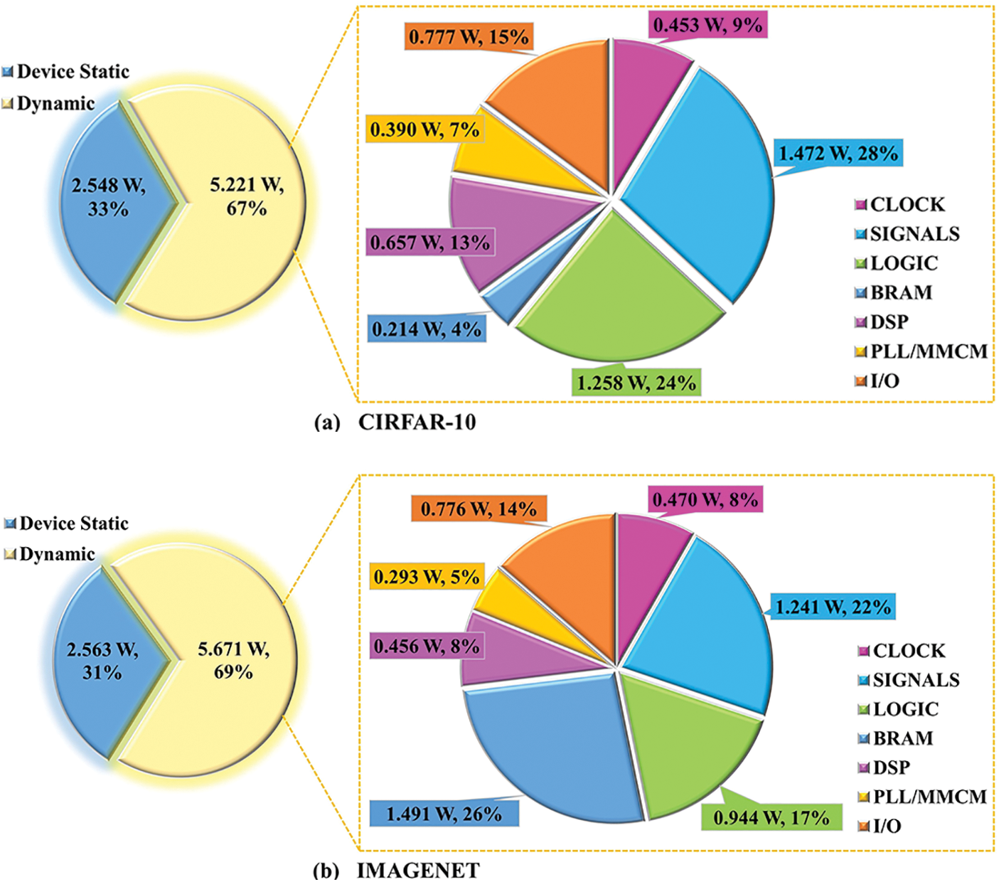
Figure 17: Power consumption of accelerators: (a) IMAGENET (b) CIRFAR-10
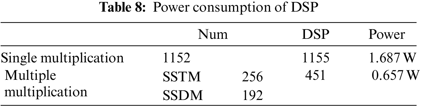
To reduce the energy consumption of logical resources and ultimately decrease the overall energy consumption of the FPGA optimized accelerator, the accelerator primarily improves the utilization of DSPs. For the multiplier, the accelerator has been custom-designed and introduces the SSTM and SSDM architectures, enabling each DSP to perform multiplication in parallel for 2–3 groups of signed data. The calculation unit of the accelerator consists of 256 SSTM and 192 SSDM, capable of parallel calculation for a total of 1152 groups of multiplication. According to the data in Table 8, it can be observed that compared to using a single DSP for multiplication, the accelerator reduces the number of DSPs by 704, thereby reducing the power consumption by 1.03 W. Since the DDR4 MIG IP invocation requires an additional 3 DSPs, the number of DSPs is 3 more than the number of multipliers.
The SSTM and SSDM architectures proposed in this article have some unique features compared to other single DSP implementations of multiple multiplication architectures. As for the SSTM structure, as can be seen from Table 9. Compared with [21], the SSTM structure can complete the multiplication of signed input data and signed output data. As for [22], SSTM consumes much less LUT and keeps the quantified data the same as actual calculation data. Moving on to the SSDM structure, the SSDM structure can support 2 different signed input data, in addition, compared with similar work in [23], the SSDM can support the calculation of higher data width of data from Table 10.


4.4 Performance Optimized by Multiplier Sharing Strategy
The accelerator chosen is VGG16 as the DCNN model for recognizing the CIFAR-10 dataset and the IMAGENET dataset. This paper customizes various parts of the FPGA optimized accelerator using the Verilog language and deploys it on the Xilinx VCU118. The recognition of the CIFAR-10 dataset and the IMAGENET dataset is evaluated using energy efficiency (GOPS/W) and DSP efficiency (GOPS/DSP) as evaluation metrics.
For CIFAR-10 dataset recognition, as shown in Table 11, when the system clock is set to 100 MHz, the FPGA optimized achieves an energy efficiency of 27.15 GOPS/W, which is 1.17 × more than [31]. The accelerator of [31] uses the pruning algorithm, and its actual calculation quantity is 62% less than that of the FPGA optimized accelerator. However, the FPGA optimized accelerator can achieve 2–3 groups of multiplication by a single DSP, so the accelerator of [31] and the accelerator of this paper have similar throughput. In addition, the accelerator of [31] uses the SSW data reading method to read the input data, but the FPGA optimized accelerator adopts the CSW data reading method, the CSW data reading method has a higher data multiplexing rate, so the FPGA optimized accelerator has a lower bandwidth requirement, which means that it has less BRAM resource consumption. Therefore, the FPGA optimized accelerator has higher energy efficiency than other accelerator. Moreover, the optimized accelerator can support a higher system clock, when the system clock is set to 200 MHz, the FPGA optimized achieves a DSP efficiency of 0.69 GOPS/DSP, which is 1.73 × more than [31]. Its energy efficiency is as high as 39.98 GOPS/W, which is 1.73 × more than [31].

For IMAGENET dataset recognition, as shown in Table 12, when the system clock is set to 150 MHz, the FPGA optimized accelerator achieves a DSP efficiency of 0.69 GOPS/DSP, which is 1.11 × −3.45 × more than [32–36]. Additionally, the accelerator has a high energy efficiency of 38.06 GOPS/W, which is 1.18 × −2.91 × more than of [33–37]. When the system clock is set to 200 MHz, although the power consumption gets higher, the increase in throughput is more significant. The FPGA optimized accelerator achieves a DSP efficiency of 0.92 GOPS/DSP, which is 1.48 × −4.6 × more than of [32–36]. What’s more, the accelerator has a high energy efficiency of 38.06 GOPS/W, which is 1.28 × −3.14 × more than [33–37]. The single DSP of the accelerator in [38] can only complete a single multiplication operation, while the single DSP of the FPGA optimized accelerator can complete an average of 2.25 multiplication operations. Therefore, even if the DSP data volume of the accelerator in [38] is 2.5 times that of the FPGA optimized accelerator, the calculation scale of the two accelerators is similar. In addition, the accelerator in [38] uses sparse coding to make its weight sparsity reach 88.3%, but the FPGA optimized accelerator only uses the quantization algorithm to compress the weight bit width by 68.8%. This means that the accelerator in [38] has lower bandwidth requirements. However, the use of the CSW data reading method reduces the bandwidth requirement of the FPGA optimized accelerator, so the FPGA optimized accelerator has higher throughput. In addition, the FPGA optimized accelerator has less DSP consumption, so it has higher energy efficiency.

With more BRAM resources and DSP resources, other accelerators may achieve higher throughput than the FPGA optimized accelerator. However, it is worth noting that each DSP unit of the FPGA optimized accelerator can perform an average of 2.55 multiplication. Additionally, by adopting the CSW data reading method, the FPGA optimized accelerator can save approximately 0.33 × the data reading time. These features make the accelerator excel in terms of energy efficiency, reaching high standards.
In this paper, the FPGA optimized accelerator architecture is proposed. To achieve the aim of improving the energy efficiency of the accelerator, the fast data readout strategy is used by the accelerator, compared with the SSW data reading method, it can reduce 33% of inference delay, and delay savings of individual channels are positively correlated with the image size. Moreover, the multiplier sharing strategy adopted by the accelerator can save 61% of the DSP resources of the accelerator, which leads to a decline in energy consumption. Finally, the DSP efficiency and energy efficiency of the accelerator are evaluated. When the system clock of the accelerator is set to 200 MHz, for the CIRFAR-10 dataset, the DSP efficiency is 0.69 GOPS/DSP, which provides 1.73 × speedup DSP efficiency over previous FPGA accelerators, and its energy efficiency is 39.98 GOPS/W, which shows 1.73 × energy efficiency compared with others. For the IMAGENET dataset, the DSP efficiency is 0.92 GOPS/DSP, which provides 1.48 × −4.6 × speedup DSP efficiency over previous FPGA accelerators, and its energy efficiency is 41.12 GOPS/W, which shows 1.28 × −3.14 × energy efficiency compared with others.
VGG16 is selected as the DCNN model for testing in this paper, but the fast data readout strategy and the multiplier sharing strategy proposed in this paper are also suitable for other neural networks, such as Resnet, MobileNet, etc., which is the focus of future work.
Acknowledgement: The authors are very grateful to the National University of Defense Technology for providing the experimental platforms.
Funding Statement: This work was supported in part by the Major Program of the Ministry of Science and Technology of China under Grant 2019YFB2205102, and in part by the National Natural Science Foundation of China under Grant 61974164, 62074166, 61804181, 62004219, 62004220, and 62104256.
Author Contributions: T. Ma and Z. Li. contributed equally to this work, the corresponding author is Q. Li. The authors confirm their contribution to the paper as follows: study conception and design: T. Ma, Z. Li and Q. Li; data collection: T. Ma and Z. Zhao; analysis and interpretation of results: Z. Li, H. Liu and Y. Wang; draft manuscript preparation: T. Ma and Z. Li. All authors reviewed the results and approved the final version of the manuscript.
Availability of Data and Materials: The data will be made publicly available on GitHub after Tuo Ma. Author completes the degree.
Conflicts of Interest: The authors declare that they have no conflicts of interest to report regarding the present study.
References
1. P. Hanh, L. Thuong and N. Sy, “FPGA platform applied for facial expression recognition system using convolutional neural networks,” Procedia Computer Science, vol. 151, pp. 651–658, 2019. [Google Scholar]
2. B. Beatriz, G. Daniel, F. Mauro, V. M. Brea and L. Paula, “Deep learning-based multiple object visual tracking on embedded system for IoT and mobile edge computing applications,” IEEE Internet of Things Journal, vol. 6, no. 3, pp. 5423–5431, 2019. [Google Scholar]
3. J. P. Bhimavarapu, S. Ramaraju, D. Nagajyothi and I. V. Rao, “Convolutional neural network based object detection system for video surveillance application,” Concurrency and Computation: Practice and Experience, vol. 35, no. 3, pp. e7461, 2023. [Google Scholar]
4. W. Krzysztof, K. Michał, W. Maciej, P. Marcin and W. Kazimierz, “Compression of convolutional neural network for natural language processing,” Computer Science, vol. 21, no. 1, 2020. [Google Scholar]
5. S. H. Khan, T. J. Alahmadi, W. Ullah, J. Iqbal, A. Rahim et al., “A new deep boosted CNN and ensemble learning based LoT malware detection,” Computers & Security, vol. 133, pp. 103385, 2023. [Google Scholar]
6. F. Abukhodair, W. Alsaggaf, A. T. Jamal, A. Sayed and R. F. Mansour, “An intelligent metaheuristic binary pigeon optimization-based feature selection and big data classification in a mapreduce environment,” Mathematics, vol. 9, no. 20, pp. 2627, 2021. [Google Scholar]
7. J. B. Lazaro, M. C. P. Po, L. M. Ramones and P. M. L. Tolidanes, “Real-time speech recognition engine for accent correction using hidden markov model,” in Proc. of EGM, Bandung, Indonesia, pp. 1–6, 2018. [Google Scholar]
8. M. T. Le, N. T. T. Thi and M. T. Vo, “Design and implementation of real time robot controlling system using upper human body motion detection on FPGA,” in 2019 IEEE Conf. ISCIT, Ho Chi Minh City, Vietnam, pp. 215–220, 2019. [Google Scholar]
9. R. F. Mansour, H. Alhumyani, S. A. Khalek, R. A. Saeed and D. Gupta, “Design of cultural emperor penguin optimizer for energy-efficient resource scheduling in green cloud computing environment,” Cluster Computing, vol. 26, no. 1, pp. 575–586, 2023. [Google Scholar] [PubMed]
10. X. Wu, Y. Ma, M. Wang and Z. Wang, “A flexible and efficient FPGA accelerator for various large-scale and lightweight CNNs,” IEEE Transactions on Circuits and Systems I: Regular Papers, vol. 69, no. 3, pp. 1185–1198, 2022. [Google Scholar]
11. L. Bai, Y. Zhao and X. Huang, “A CNN accelerator on FPGA using depthwise separable convolution,” IEEE Transactions on Circuits and Systems II: Express Briefs, vol. 65, no. 10, pp. 1415–1419, 2018. [Google Scholar]
12. F. Tu, S. Yin, O. Peng, S. Tang, L. Liu et al., “Deep convolutional neural network architecture with reconfigurable computation patterns,” IEEE Transactions on Very Large Scale Integration (VLSI) Systems, vol. 25, no. 8, pp. 2220–2233, 2017. [Google Scholar]
13. S. Han, J. Pool, J. Tran and W. J. Dally, “Learning both weights and connections for efficient neural networks,” in Proc. of NIPS’15, Montreal, Canada, pp. 1135–1143, 2015. [Google Scholar]
14. W. Cheng, I. Lin and Y. Shih, “An efficient implementation of convolutional neural network with CLIP-Q quantization on FPGA,” IEEE Transactions on Circuits and Systems I: Regular Papers, vol. 69, no. 10, pp. 4093–4102, 2022. [Google Scholar]
15. B. Zhuang, C. Shen, M. Tan, L. Liu and I. Reid, “Towards effective low-bitwidth convolutional neural networks,” in Proc. of the IEEE Conf. on Computer Vision and Pattern Recognition (CVPR), Salt Lake City, UT, USA, pp. 7920–7928, 2018. [Google Scholar]
16. J. Wang, J. Lin and Z. Wang, “Efficient hardware architectures for deep convolutional neural network,” IEEE Transactions on Circuits and Systems I: Regular Papers, vol. 65, no. 6, pp. 1941–1953, 2018. [Google Scholar]
17. J. Lu, D. Liu, X. Cheng, L. Wei, A. Hu et al., “An efficient unstructured sparse convolutional neural network accelerator for wearable ECG classification device,” IEEE Transactions on Circuits and Systems I: Regular Papers, vol. 69, no. 11, pp. 4572–4582, 2022. [Google Scholar]
18. Z. Liu, Y. Dou, J. Jiang and J. Xu, “Automatic code generation of convolutional neural networks in FPGA implementation,” in 2016 IEEE Conf. FPT, Xi’an, China, pp. 61–68, 2016. [Google Scholar]
19. Y. Ma, Y. Cao, S. Vrudhula and J. Seo, “Optimizing the convolution operation to accelerate deep neural networks on FPGA,” IEEE Transactions on Very Large Scale Integration (VLSI) Systems, vol. 26, no. 7, pp. 1354–1367, 2018. [Google Scholar]
20. P. Haghi, M. Kamal, A. Ali and M. Pedram, “O4-DNN: A hybrid DSP-LUT-based processing unit with operation packing and out-of-order execution for efficient realization of convolutional neural networks on FPGA devices,” IEEE Transactions on Circuits and Systems I: Regular Papers, vol. 67, no. 9, pp. 3056–3069, 2020. [Google Scholar]
21. S. Lee, D. Kim, D. Nguyen and J. Lee, “Double MAC on a DSP: Boosting the performance of convolutional neural networks on FPGAs,” IEEE Transactions on Computer-Aided Design of Integrated Circuits and Systems, vol. 38, no. 5, pp. 888–897, 2019. [Google Scholar]
22. E. Kalali and V. L. Rene, “Near-precise parameter approximation for multiple multiplications on a single DSP block,” IEEE Transactions on Computers, vol. 71, no. 9, pp. 2036–2047, 2022. [Google Scholar]
23. T. Han, Convolutional Neural Network with INT4 Optimization on Xilinx Devices. San Jose, CA, USA, 2020. [Online]. Available: https://docs.xilinx.com/v/u/en-US/wp521-4bit-optimization (accessed on 01/10/2023) [Google Scholar]
24. Z. Li, B. Ni, X. Yang, W. Zhang and W. Gao, “Residual quantization for low bit-width neural networks,” IEEE Transactions on Multimedia, vol. 25, pp. 214–227, 2023. [Google Scholar]
25. K. Simonyan and A. Zisserman, “Very deep convolutional networks for large-scale image recognition,” in Int. Conf. on Learning Representations 2015, San Diego, CA, USA, 2015. [Google Scholar]
26. A. Krizhevsky, I. Sutskever and G. E. Hinton, “ImageNet classification with deep convolutional neural networks,” Communications of the ACM, vol. 60, pp. 84–90, 2012. [Google Scholar]
27. R. Banner, Y. Nahshan and D. Soudry, “Post training 4-bit quantization of convolutional networks for rapid-deployment,” in Proc. of NIPS’19, Red Hook, NY, USA, pp. 7950–7958, 2019. [Google Scholar]
28. S. Jung, C. Son, S. Lee, J. Son, J. Han et al., “Learning to quantize deep networks by optimizing quantization intervals with task loss,” in 2019 IEEE Conf. on CVPR, Long Beach, CA, USA, pp. 4345–4354, 2019. [Google Scholar]
29. Y. Choukroun, E. Kravchik, F. Yang and P. Kisilev, “Low-bit quantization of neural networks for efficient inference,” in 2019 IEEE Conf. on ICCVW, Seoul, Korea, pp. 3009–3018, 2019. [Google Scholar]
30. J. Choi, Z. Wang, S. Venkataramani, P. I. Chuang, V. Srinivasan et al., “PACT: Parameterized clipping activation for quantized neural networks,” arXiv:1805.06085, 2018. [Google Scholar]
31. W. Pang, C. Wu and S. Lu, “An energy-efficient implementation of group pruned CNNs on FPGA,” IEEE Access, vol. 8, pp. 217033–217044, 2020. [Google Scholar]
32. T. Yuan, W. Liu, J. Han and F. Lombardi, “High performance CNN accelerators based on hardware and algorithm co-optimization,” IEEE Transactions on Circuits and Systems I: Regular Papers, vol. 68, no. 1, pp. 250–263, 2021. [Google Scholar]
33. C. Zhu, K. Huang, S. Yang, Z. Zhu, H. Zhang et al., “An efficient hardware accelerator for structured sparse convolutional neural networks on FPGAs,” IEEE Transactions on Very Large Scale Integration (VLSI) Systems, vol. 28, no. 9, pp. 1953–1965, 2020. [Google Scholar]
34. L. Gong, C. Wang, X. Li, H. Chen and X. Zhou, “MALOC: A fully pipelined FPGA accelerator for convolutional neural networks with all layers mapped on chip,” IEEE Transactions on Computer-Aided Design of Integrated Circuits and Systems, vol. 37, no. 11, pp. 2601–2612, 2018. [Google Scholar]
35. K. Guo, L. Sui, J. Qiu, J. Yu, J. Wang et al., “Angel-eye: A complete design flow for mapping CNN onto embedded FPGA,” IEEE Transactions on Computer-Aided Design of Integrated Circuits and Systems, vol. 37, no. 1, pp. 35–47, 2018. [Google Scholar]
36. Y. Chen, J. He, X. Zhang, C. Hao and D. Chen, “Cloud-DNN: An open framework for mapping DNN models to cloud FPGAs,” in Proc. of FPGA’2019, New York, NY, USA, pp. 73–82, 2019. [Google Scholar]
37. Q. Xiao and Y. Liang, “Zac: Towards automatic optimization and deployment of quantized deep neural networks on embedded devices,” in 2019 IEEE Conf. on ICCAD, Westminster, CO, USA, pp. 1–6, 2019. [Google Scholar]
38. L. Lu, J. Xie, R. Huang, J. Zhang, W. Lin et al., “An efficient hardware accelerator for sparse convolutional neural networks on FPGAs,” in 2019 IEEE Conf. on FCCM, San Diego, CA, USA, pp. 17–25, 2019. [Google Scholar]
Cite This Article
 Copyright © 2023 The Author(s). Published by Tech Science Press.
This work is licensed under a Creative Commons Attribution 4.0 International License , which permits unrestricted use, distribution, and reproduction in any medium, provided the original work is properly cited.
 Downloads
 Citation Tools