
 Submit a Paper
 Propose a Special lssue
 Open Access
ARTICLE

Optimization of Quantum Cost for Low Energy Reversible Signed/Unsigned Multiplier Using Urdhva-Tiryakbhyam Sutra
1 Benha Faculty of Engineering, Benha University Benha, Egypt
2 Arab Academy for Science, Technology and Maritime Transport-Arab League Cairo, Egypt
* Corresponding Authors: Marwa A. Elmenyawi. Email: ,
Computer Systems Science and Engineering 2023, 46(2), 1827-1844. https://doi.org/10.32604/csse.2023.036474
Received 01 October 2022; Accepted 14 December 2022; Issue published 09 February 2023
 View Full Text
 Download PDF
Abstract
One of the elementary operations in computing systems is multiplication. Therefore, high-speed and low-power multipliers design is mandatory for efficient computing systems. In designing low-energy dissipation circuits, reversible logic is more efficient than irreversible logic circuits but at the cost of higher complexity. This paper introduces an efficient signed/unsigned 4 × 4 reversible Vedic multiplier with minimum quantum cost. The Vedic multiplier is considered fast as it generates all partial product and their sum in one step. This paper proposes two reversible Vedic multipliers with optimized quantum cost and garbage output. First, the unsigned Vedic multiplier is designed based on the Urdhava Tiryakbhyam (UT) Sutra. This multiplier consists of bitwise multiplication and adder compressors. Compared with Vedic multipliers in the literature, the proposed design has a quantum cost of 111 with a reduction of 94% compared to the previous design. It has a garbage output of 30 with optimization of the best-compared design. Second, the proposed unsigned multiplier is expanded to allow the multiplication of signed numbers as well as unsigned numbers. Two signed Vedic multipliers are presented with the aim of obtaining more optimization in performance parameters. DesignI has separate binary two’s complement (B2C) and MUX circuits, while DesignII combines binary two’s complement and MUX circuits in one circuit. DesignI shows the lowest quantum cost, 231, regarding state-of-the-art. DesignII has a quantum cost of 199, reducing to 86.14% of DesignI. The functionality of the proposed multiplier is simulated and verified using XILINX ISE 14.2.Keywords
Nomenclature
| B2C | Binary to two’s Complement |
| C | Carry |
| CI | Constant Inputs |
| DFG | Double Feynman gate |
| FA | Full Adder |
| FG | Feynman gate |
| GO | Garbage Outputs |
| HA | Half Adder |
| K | Boltzmann constant |
| LSB | Least Significant Bit |
| MSB | Most Significant Bit |
| MUX | Multiplexer |
| NG | New Gate |
| PG | Peres Gate |
| QC | Quantum Cost |
| S | Sum |
| T | Temperature |
| TG | Toffoli Gate |
| UT | Urdhava Tiryakbhyam |
The demand for high-performance systems has been increasing due to the development of signal processing, machine learning, and many digital aspects. Moreover, since multiplication is crucial in many applications, optimizing the multiplication circuit design is essential. Power dissipation is a challenging issue in designing digital/electronic circuits. Multipliers are considered one of the primary sources of power dissipation in any system. Using reversible circuits is one of the feasible solutions to reduce power dissipation [1]. Reversible logic gates are the gates where every input is mapped to an output; hence they are NxN gates.
Multipliers play an essential role in any computing or processing, or system. Multipliers are utilized in various digital signal processing applications such as wavelet compression, FFT, digital filtering, ALU, and image processing. It is essential to employ a faster multiplier to improve the system performance, as the system performance is primarily based on the multiplier unit performance. The Vedic multiplier is one such multiplier that outperforms traditional multipliers while having a lower latency.
The Vedic multiplier depends on Vedic mathematics, which consists of 16 Sutras. One of these Sutras is the UT which means “vertical and crosswise.” The multiplication process starts vertically and then moves to crosswise multiplication. The design of the N × N Vedic multiplier is performed using two design approaches. The first approach is to design a 2 × 2 Vedic multiplier using vertical and crosswise multiplication and generate its equations. Then use the Karatsuba methodology to build the 4 × 4 Vedic multiplier using 2 × 2 multiplier blocks and design an 8 × 8 multiplier using 4 × 4. The second approach is to develop the N × N multiplier using the “vertical and crosswise” multiplication for all the N-bits and generate 2N equations. Each equation constitutes the direct addition of the product terms generated from the bitwise multiplication.
With the need to implement a low-power, high-performance system, merging the low-power benefit of reversible architecture with the extraordinarily fast speed of the Vedic multiplier is important. In this paper, we propose the design of a reversible 4 × 4 Vedic multiplier that uses the generation of 8 equations for the multiplication process. To the best of our knowledge, this is the first reversible design using this approach. Unfortunately, Vedic multipliers are unsigned, generating incorrect output if the multiplier and/or multiplicand inputs are a signed number. Therefore, when using a Vedic multiplier with signed inputs, it is essential to convert the negative numbers to positive numbers and then perform the multiplication process using a Vedic multiplication. Finally, adjust the output sign according to the sign of the inputs. This methodology is explained and designed in traditional logic in previous research [2].
The main objective of this paper is to design a signed/unsigned 4 × 4 reversible Vedic multiplier with minimum quantum cost to reduce the energy dissipation and the design complexity. A binary two’s complement circuit and multiplexers (MUX) are used to adjust the sign of the inputs and outputs for signed numbers multiplication. The article presents the first implementation of a reversible signed/unsigned Vedic multiplier to the best of our knowledge.
The contribution of this paper can be summarized as follows:
• Implementation of minimum quantum cost, garbage output, and TRLIC unsigned 4 × 4 reversible Vedic multiplier design.
• An optimized reversible 4-bit binary 2’s complement circuit is designed. Moreover, a generic n-bit binary 2’s complement circuit is proposed.
• A reversible 4 × 4 signed/unsigned Vedic multiplier is proposed using the designed unsigned multiplier, the binary 2’s complement circuit, and MUXs to choose between the signed or unsigned cases.
• Furthermore, this design is optimized by merging the binary 2’s complement circuit with the MUX circuit. We introduced a generic n-bit merged B2C and MUX circuit, which reduces the Quantum Cost of the multiplier design.
The rest of this paper is organized as follows: Section 2 provides background on the reversible logic circuits, the UT sutra, and adder compressors, while Section 3 reviews the related work. Section 4 describes our proposed design of an unsigned Vedic multiplier, while Section 5 introduces the combined multiplier for signed and unsigned. The results and analysis of the proposed multipliers are presented in Section 6, along with the comparison of related designs. Finally, the paper is concluded in Section 7.
Power consumption is considered the bottleneck in developing large, complex, and high-speed designs. Landauer [3] proved that there is energy dissipation in traditional logic circuits. The energy loss is directly proportional to the lost bits of information during the circuit operation. The thermal energy loss is up to kTln2, where K = 1.3806505 × 10⁻²³ J/K is the Boltzmann constant, and T is the environment’s temperature around the circuit operation [4,5]. Although this looks to be a modest quantity of energy, the dissipated energy can be enormous when considering the whole CPU, which has millions of transistors. However, if the system can return from its final state to its initial state, it consumes no energy and theoretically functions as a lossless system. Bennett [6] proved that reversible circuits could avoid the energy dissipation of kT ln2 because there is no loss of information. Reversible logic circuits have the following characteristics [7–9]:
• No fanout or feedback is allowed.
• They have a one-to-one correspondence between inputs and outputs.
• Constant inputs (CI) are the inputs to a reversible circuit that are kept at a constant value of 0 or 1 to achieve the required functionality.
• Garbage Outputs (GO) are unused outputs in further computation.
• Quantum Cost (QC) is the sum of the quantum cost of the gates that constitutes the design. The 1 × 1 gate has a quantum cost of 0, while each 2 × 2 gate has a quantum cost of 1.
• Total Reversible Logic Implementation Cost (TRLIC) is the sum of the constant inputs, garbage outputs, quantum cost, and the number of gates.
When designing a circuit using reversible gates, it is required to reduce the garbage output, therefore, reducing the energy loss. Also, it is recommended to reduce the constant input and the quantum cost. It is challenging to optimize the reversible circuit, and there is much research to perform that task. Reversible circuits have many applications, such as quantum computing, nanotechnology, and low-power systems.
Reversible gates are used to implement reversible circuits with the mentioned characteristics. Several reversible gates were introduced in the past several years through the literature; below is the investigation of some reversible gates.
• Feynman Gate: A 2 × 2 Feynman gate (FG), known as controlled-NOT, has two inputs and two outputs, as shown in Fig. 1a. It is frequently utilized for fanout purposes, and its quantum cost equals one.
• Toffoli Gate: Toffoli gate (TG) is a 3 × 3 reversible gate known as a “Controlled-Controlled Not gate (CCNOT), shown in Fig. 1b. In a TG, the third input is complemented when the first two inputs are connected to 1; otherwise, it remains the same. TG has a quantum cost of 5.
• Peres Gate: Peres gate (PG) shown in Fig. 1c has three inputs and outputs. A PG consists of one Feynman gate and one Tofolli gate. The Quantum cost of PG is four.
• SAM Gate: A 3 × 3 SAM gate has three inputs and three outputs, as shown in Fig. 1d, and its quantum cost is equal to four. It can obtain three operations if the last input is set to zero. The first operation complements one of its inputs, while the second is AND between the first two inputs. Finally, the last operation is an OR operation between these two inputs.
• BME Gate: The BME gate was introduced in [10]. It is a 4 × 4 reversible gate, as illustrated in Fig. 1e. The quantum cost of a BME gate is 5.
• RMUX Gate: A 3 × 3 RMUX gate has three inputs and three outputs, as introduced in Fig. 1f. It can be used as a 2 × 1 MUX by connecting the first input to the selector and the MUX inputs to the second and third inputs of the RMUX gate. The output of the MUX is the gate’s second output, and the rest of the outputs are considered garbage outputs. It has a quantum cost of four.
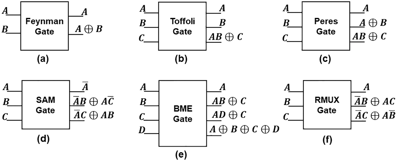
Figure 1: Reversible gates examples
Vedic Mathematics is an ancient system that provides efficient calculations in engineering and science fields. Vedic mathematics consists of 16 sutras for different problems. One of the most known sutras is the UT; it is used in multiplying two numbers of any number of digits and in any numbering system. The multiplication process starts in the vertical direction and then moves crosswise multiplication, hence its name “Vertical and Crosswise” [11,12]. The significant advantage of Vedic mathematics is its simplicity, therefore implementing them using less complex and low-power circuits. In other multiplying algorithms like Booth and array multipliers, the multiplication process latency increases proportionally with increasing the inputs’ length. However, increasing the inputs’ size in the Vedic multiplier does not increase the multiplication process latency [5]. Moreover, Vedic multipliers improve the performance concerning the processing time because they require fewer adders than other multiplication methods [13].
There are two approaches to designing a 4 × 4 Vedic Multiplier. The first approach is to use the Karatsuba divide and conquer algorithm. First, split the multiplicand and multiplier into two groups, 2-bits in each, then use 2 × 2 Vedic multipliers generating four partial products. Finally, use three 4-bits binary adders to add the partial products, as shown in Fig. 2 [1,13].

Figure 2: 4 × 4 Vedic multiplier using four 2 × 2 multipliers
The second approach uses the UT sutra directly shown in Fig. 3. It generates the system of equations (Eq. (1) to Eq. (8)). The generation of product terms is similar to the product terms generation in the array multiplier. The difference is that the product terms are added concurrently instead of generating partial products and adding them by n-bit binary adders [2].

Figure 3: Steps of 4 × 4 multiplication using Vedic mathematics
The following equations of 4 × 4 Vedic are concluded using this mechanism illustrated in Fig. 3 and following the same steps as in [14].
Full adders are used to add three bits simultaneously, generating the result in two bits sum and carry. As shown in Eqs. (1)–(8) of UT, some equations require four bits addition (Eqs. (3), (6)), and others require the addition of five bits (Eqs. (4), (5)). Adder compressors are used to perform the addition of more than three bits [14,15]. Adding four or five bits generates the result in three bits sum, carry 0, and carry 1.
A 4:3 adder compressor is designed to add 4 bits, as shown in Fig. 4a. The circuit consists of a full adder and two half adders to implement Eqs. (9)–(11). Likewise, we need to add 5 bits, so a 5:3 adder compressor is utilized. This compressor uses two full adders and a half-adder, as presented in Fig. 4b.

Figure 4: Adder compressors
Much research has been proposed for the Vedic multiplier in both irreversible and reversible logic. In the irreversible logic, some designs built on the first approach using the Karatsuba algorithm, while others built on the second approach using the system of equations. In reversible logic, most research depends on the first approach, to the best of our knowledge. Ariafar et al. [1] proposed two 4 × 4 Vedic multiplier designs depending on the first Vedic multiplication approach. They used ripple-carry adders to implement the three required 4-bit adders. Their second design introduced a parity-preserved multiplier that employed a 2 × 2 parity-preserved Vedic multiplier and parity-preserved adders. However, this design suffers from a high TRLIC of about 279, mainly from a high quantum cost that equals 162. Rashno et al. [5] proposed a low-power 4 × 4 reversible Vedic multiplier. First, they introduced a 2 × 2 multiplier in four designs to reduce the gate count and quantum cost. Then the authors proposed a 4 × 4 multiplier using the four 2 × 2 multiplier building blocks. Finally, the authors proposed a general formula to extend the multiplier to the N × N multiplier. Although their design provided a lower quantum cost than the designs in the literature, it is still considered high. The reduction was only a quantum cost of 2 (from 162 of the literature design to 160). Awade et al. [13] provided a comparative study between three designs for 8 × 8 reversible. Each of them was implemented using different adders to study the impact of adder type on the multiplier circuit. The designed adders are ripple-carry, carry skip, and carry select adders. Although the multiplier designed with the ripple carry adders utilized the highest area, it provided the minimum number of reversible gates and the lowest garbage outputs design. The multiplier design used carry select adders utilized the minimum area with the minimum power dissipation. However, it was implemented using the highest number of reversible gates and garbage outputs. Swathi et al. [16] proposed six different reversible Vedic multiplier architectures for 2 × 2, 4 × 4, 8 × 8, and 16 × 16. They designed the multiplier N × N using the blocks of the M × M where M = N/2. The main shortcomings of the literature studies are high quantum cost, and the lack of handling the multiplication of signed numbers using Vedic multiplier.
The Vedic multiplier is used to multiply unsigned numbers. There are different methods to utilize the multiplication for signed number multiplication, such as Booth, Baugh Wooley, and Wallace tree. Nagamani et al. [17] presented a reversible radix-4 booth multiplier that can be used as signed or unsigned. They designed the multiplier based on three units: control, arithmetic, and MUX units. The control unit generates three signals: A, S, and M, where A equals one if it is required to perform an arithmetic operation by the arithmetic unit. The arithmetic unit performs two operations, addition, and subtraction, based on the S signal. Finally, the MUX unit was selected to perform one shift depending on the M value. This paper optimized the garbage outputs and ancillary input at the expense of quantum cost. Barati [18] implemented three 32 × 32 multipliers: Vedic mathematics, Baugh Wooley, and Wallace tree. Three different methods were proposed to design a ripple carry adder with 16 × 16 Vedic multipliers to produce a 32 × 32 multiplier without details about the design of the multiplier. Also, this paper didn’t compare with the state of the art in that field to analysis the performance parameter such as CI, GO and QC. PourAliAkbar et al. [19] proposed four parity-preserving reversible multiplier circuits. The first two circuits multiply unsigned numbers with size 4 × 4 and extended to N × N while the last two circuits are utilized with signed numbers with size 5 × 5 and extended to N × N. They divided the design to two parts: partial product generation and partial product addition. They proposed three blocks which used to output multiplication and addition of the bits depending on the setting of inputs. This paper optimized the CI, GO and QC but they didn’t combine the two multipliers, signed and unsigned, in one circuit. Raveendran et al. [20] proposed 8 × 8 signed Baugh-Wooley Wallace tree multiplier using inexact, exact compressors, half adders, and full adders. All these blocks were implemented using reversible logic. This paper introduced only signed multiplier.
4 The Proposed 4 × 4 Unsigned Vedic Multiplier
A 4 × 4 Vedic multiplier design is proposed using the system of equations (Eq. (1) to Eq. (8)) approach. This approach needs the generation of product terms, a direct AND gate between one bit of the multiplier input to its corresponding bit of the multiplicand, and then adding these product terms. Some equations can be implemented simply using half adder (Eqs. (2), (8)) or full-adder circuits (Eq. (7)). While other equations should be realized using adder compressors since the number of bits to be added is more than three bits (Eq. (3) to Eq. (6)). The block diagram of the proposed design is illustrated in Fig. 5. This block diagram does not include the generation of the product terms since it is implemented by an AND gate to generate the sixteen product term from

Figure 5: The block diagram of the proposed unsigned 4 × 4 Vedic multiplier
Product terms are bitwise multiplication between a bit from the multiplier input and a bit from the multiplicand input, implemented logically by an AND gate. For example, a 4 × 4 Vedic multiplier requires 16 product terms. Therefore, the BME gate generates the product terms, as illustrated in Fig. 6. The main advantage of using the BME gate is that a gate can generate two product terms and hence reduce the total number of required gates from 16 to 8 gates. Each BME gate has one constant input (input C shown in Fig. 1e is attached to 0). The first output of each gate in Fig. 6a is fed to the first input of its corresponding input in Fig. 6b. The total garbage output of the bitwise multiplication circuit is 11.
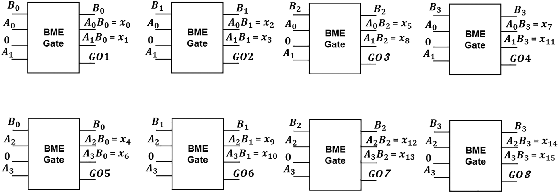
Figure 6: Bitwise multiplication to generate the product terms
Half adder circuit can be implemented using a Peres gate by connecting the third input of a PG (the input C) to 0, as illustrated in Fig. 7. The PG gate is used to implement all the half adders shown in Fig. 5 except for the last half adder. The last half adder implements Eq. (8), where the carry result is neglected. So, an FG is used instead of the PG to reduce the quantum cost.

Figure 7: Peres gate as a half adder and its quantum realization
Many reversible full-adder circuits have been designed in the last years [21–24], and each design tries to improve the performance of the adder circuit. This paper adopts the full adder in [22] illustrated in Fig. 8. This circuit is used to implement the standalone full adder shown in Fig. 5 and implement the full-adder circuits needed in 4:3 adder compressors and 5:3 adder compressors shown in Fig. 4.

Figure 8: The block diagram of the reversible full adder and its quantum realization
4.3 Reversible Unsigned 4 × 4 Vedic Multiplier
The proposed unsigned 4 × 4 Vedic multiplier shown in Fig. 5 is implemented using the reversible gates explained in the previous subsections. The quantum realization of the proposed 4 × 4 Vedic multiplier is illustrated in Fig. 9.

Figure 9: The quantum realization of the proposed 4 × 4 unsigned Vedic multiplier
5 Signed/Unsigned Reversible Vedic Multiplier
A Vedic Multiplier is an unsigned multiplier. In order to convert it to a signed multiplier, there are two approaches; the first one is to use the multiplier design in Fig. 2, but instead of using 2 × 2 Vedic multipliers, use Booth multipliers. The Booth multiplier can multiply both signed and unsigned numbers. However, the disadvantage of this method is that it is not scalable easily. For example, an 8 × 8 signed Vedic multiplier uses 4 × 4 Booth multipliers blocks instead of 2 × 2. Similarly, designing a 16 × 16 Vedic multiplier requires 8 × 8 Booth multipliers, creating new blocks for each expansion.
The second approach is to use the rule of signed numbers multiplication. When multiplying two positive or negative numbers, the result is the positive multiplication of the inputs. In contrast, when multiplying dislike sign numbers, the result would be the negative of multiplying the positive inputs.
The second technique is used in [2]. The advantage of this technique is that Vedic Multiplier can be expanded for the required number of input digits, then use the appropriate 2’s complement circuit and a mux to select between the signed/unsigned and positive/negative numbers. Also, there is no restriction on building the N × N Vedic multiplier; it can be implemented using the system of equations or from four N/2 Vedic multipliers. This approach is illustrated in Fig. 10.
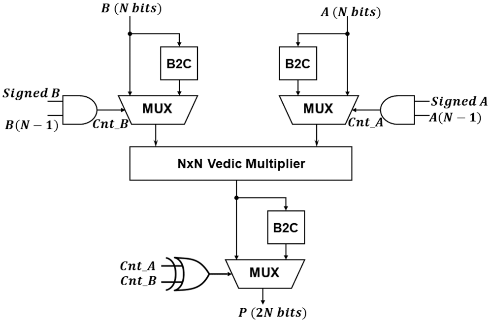
Figure 10: Signed/Unsigned Vedic multiplier proposed in [2]
It is required to use an efficient binary two’s complement circuit, MUX, and the proposed Vedic multiplier circuit to realize the design in Fig. 10 using reversible logic. In the following subsections, we will introduce two designs to the Signed/Unsigned Vedic Multiplier. We seek to reduce the quantum cost and garbage output.
5.1 Signed/Unsigned Proposed DesignI
The Signed/Unsigned Vedic multiplier consists of B2C (4-bit and 8-bit) and 2 × 1 MUXs. In the first proposed design, we introduced a new design for the B2C to reduce the quantum cost compared to previous research and make it easier to be extendible.
There are different ways to represent a negative number; Signed magnitude, 1’s complement, and 2’s complement. The 2’s complement representation is considered the best way to represent the negative numbers for the following reasons.
• In the subtraction with complements method, only one addition is required if the 2’s complement is used, while using the 1’s complement requires two additions because of the end carry addition.
• The 1’s complement representation has two representations for zero.
As introduced in [25,26], there are different implementations for 2’s complement circuit. To the best of our knowledge, the design in [25] has the minimum quantum cost [11] for 4-bit. They used two NG and one FG gate. Our proposed B2C achieved 9 QC, which outperformed the previous design. Furthermore, the 8-bit B2C using this procedure outperforms the B2C implementation in [25] in the QC as our 8-bit B2C needs 25 while their design requires 31.
For a B2C circuit with A, B, C, and D are the inputs while W, X, Y, and Z are the outputs, Karnaugh maps are used to simplify and generate the equations:

Figure 11: The reversible B2C (a) 4-bit B2C (b) n-bit B2C circuit
To extend the B2C to 5 bits, the third input of the last PG gate is connected to zero and use one more PG gate. The added PG gate has three inputs; the first input is the last output of the previous PG gate, and the two inputs are the most significant two bits of the input number. The outputs of the second PG gate are one garbage output and the last two outputs of the 2’s complement of the input. To have generic B2C, the last PG should have the third input connected to zero, and the third output should be connected to one more PG gate. The added PG gate has one input from the previous PG gate, and the other two inputs are the two bits of original input from the left. The generic N-bit B2C is introduced in Fig. 11b.
The second part of our design uses MUX to select between the input number or its 2’complement. To the best of our knowledge, the best implementation for MUX 2 × 1 is the RMUX gate shown in Fig. 1f, which has QC equal to 4. The input number and its complement consist of four bits, while the Vedic multiplier output consists of eight. The number and its complement have a common LSB equal to the bit itself, while the difference begins afterwards. Therefore, six 2 × 1 MUX are needed to select between the numbers (multiplicand and multiplied) and their complement in part preceding the Vedic multiplier. In part following the Vedic, seven 2 × 1 MUX are needed to select between the result and its complement. Therefore 13 RMUX gates are required for the first proposed design.
Since the reversible circuit does not permit the use of the output more than once, we need a fanout generator circuit to use the output more than once. Different gates can be used as fanout generators, such as FG, DFG, and BVF. The FG results in two copies of the input if the second input is connected to zero, while the DFG generates three copies of the input if the second and third inputs are cleared. Depending on the connections, the BVF can generate two copies of two different inputs or four copies of the same input. In the first case, if the first and third inputs of BVF are connected to the two different inputs while the other inputs are connected to zero, we obtain two copies of the first input on the first two outputs. The copies of the second input are introduced in the third and fourth outputs. While in the second case, if we connect the first and third inputs of the BVF gate to the same input, we generate four copies of the same input.
The proposed design requires a fanout generator between the multiplicand out from the MUX and Vedic multiplier. Also, the design needs a fanout generator following the Vedic multiplier to generate two copies of the Vedic result. There is no need to use a fanout circuit for multiplier input as the Vedic generates different copies from the BME gate. We need four copies of the last three bits of the multiplicand. There are various options to generate four copies of input; the best option is to use one BVF, three DFG, and one FG gate, which leads to the minimum number of gates. We connect the A1 and A2, the second and third bits of the multiplicand, to the first and third input of BVF and connect the first output of BVF to the first input of DFG to obtain another two copies. Also, A2 is connected to another DFG gate to get its other three copies. Finally, A3 is connected to the first input of FG and connects its first output to the DFG gate to generate three more copies. Moreover, we need seven FG gates to generate two copies of the last seven bits of Vedic output.
5.2 Signed/Unsigned Proposed DesignII
We propose a new design that combines the B2C and MUX in one circuit, intending to reduce the quantum cost. Fig. 12 introduced the four-bit combined B2C with a 2 × 1 MUX. We add one more SAM gate to the B2C circuit presented in Fig. 11a to give the option to choose between the LSB of the input or logic one, depending on the selector. The zero value of the selector chooses the LSB if 2’complement is required. While to get the original input, logic one is chosen by the one value of the selector. If the output is the LSB, the circuit works as B2C explained in the previous section. If the SAM1 gate outputs logic one in its second output connected to the second input of the SAM2 gate (the first gate in B2C in the previous design), this input equals one. In this case, the second output of the SAM2 gate produces Logic one (1 OR the second LSB input), which is then complemented and fed to the first input of the PG gate. The last two inputs of the PG gate are generated from the DFG gate to select the input or its complement. Finally, the last two outputs of the PG gate are the circuit’s final outputs which equal the original inputs. These outputs are the output of XOR, where its inputs are logic zero and the input itself. The second output has to be controlled to obtain the correct expression if the selector equals one. In that case, the obtained output is

Figure 12: The four-bit merged B2C with MUX
This circuit can be easily extended as we add one PG and one FG gate for every added bit except for the last two MSBs of the input. For these bits, we use only one PG, not two gates, and one DFG instead of the FG gates to reduce the quantum cost and the number of gates. For the following added PG gate, the first input is the last output of the previous PG gate, and the second input is from the FG gate, where its input is the extended bit and selector. The last input of this PG is logic zero. The last PG gate in the extended circuit resembles the last PG gate introduced in Fig. 12. The merged B2C with MUX eliminates the need for a fanout generator for the result of the Vedic multiplier as we no longer need two copies of the result to be the inputs to B2C and MUX.
The proposed 4 × 4 unsigned Vedic multiplier shown in Fig. 5 and the signed/unsigned Vedic multiplier shown in Fig. 10 are verified using XILINX ISE 14.2. The design codes are written in VHDL language and then compiled, tested, and simulated. The simulation area is divided into four regions, as shown in Fig. 13. The signed_a and the signed_b control inputs are set to 1 for sign multiplication in the first three regions. In the last region, they are set to 0 for unsigned multiplication. Region A illustrates the multiplication of two positive signed numbers. While region B demonstrates the multiplication of one signed positive number, and the other one is a negative number. Region C shows the result of multiplying two signed negative numbers. The last region, Region D, illustrates the multiplication of unsigned numbers.

Figure 13: Simulation results
6.1 Results of the Unsigned 4 × 4 Vedic Multiplier
The results of the proposed unsigned 4 × 4 Vedic multiplier shown in Fig. 5 are represented in Table 1. The first three columns of Table 1 represent the reversible characteristics of each gate, and then the utilized number of each gate is shown in column 4. The last three columns denote the reversible gate characteristics for the utilized gates of the whole multiplier design, and the design characteristics are summarized in the last row. Finally, the results of the proposed multiplier compared to the previous work are provided in Table 2 and are illustrated in Fig. 14.


Figure 14: Comparison of 4 × 4 unsigned Vedic multiplier with previous work
Design in [16] is considered the best in the literature regarding QC, CI, gate count and TRLIC. In contrast, the design provided in [5] is regarded as the best literature design in the GO. The proposed 4 × 4 unsigned Vedic multiplier is superior to the previous designs in terms of the different figures of merit. Table 2 explores the reduction of the reversible design characteristics of the proposed design. The quantum cost is reduced to 94% of the design in [16], and a total TRLIC reduction to 90.3%. This reduction is because the design of 4-bit binary adders utilizes more gates and generates more garbage outputs than compressor adders. Hence, it is apparent that concurrently adding the product terms is more efficient than producing all the partial products and then using a 4-bits binary adder to add them.
Despite designing the Vedic multiplier using the equations approach provided the minimum number of gates, quantum cost, and TRLIC, this method is efficient for 2 × 2 and 4 × 4 multipliers; more than an 8 × 8 multiplier will require more complex compressors and increase the delay and complexity. For example, the 8 × 8 multiplier equations in [28] require the addition of 8 terms simultaneously (hence the need for an 8:4 compressor). Moreover, the equations of the 16 × 16 multiplier in [29,30] require the addition of 19 terms simultaneously, leading to the use of very complex cascaded compressors and adders that will increase the delay.
6.2 Results of the Signed/Unsigned 4 × 4 Vedic Multiplier
We introduced two designs for signed/unsigned Vedic multipliers in this paper. The first design constitutes the proposed B2C circuit, the RMUX gate, and the proposed unsigned Vedic multiplier in Fig. 9. This design is refined with the merged B2C and MUX circuits in the proposed DesignII.
A B2C circuit is used in DesignI to allow the multiplication of signed numbers using the Vedic multiplier. The proposed 4-bits B2C circuit shown in Fig. 11a is compared with other B2C designs, as shown in Table 3. The improvement percentage compared to [25] regarding QC is the reduction to 81.82%. The proposed design outperforms the previous work in terms of quantum cost but not in terms of CI and GO. A generic n-bit B2C is also proposed; we propose a generic equation to calculate the quantum cost of any n-bit B2C as

One of the most important of evaluating a reversible circuit is quantum cost. The first design has a quantum cost of 231. This design consists of two 4-bit B2C, two AND gates, 13 2 × 1 MUX, the proposed unsigned Vedic multiplier, one 8-bit B2C, one XOR, and two fanout generators for both the multiplicand and result of the Vedic. The quantum cost for each part is 2 × 9, 2 × 4, 13 × 4, 111, 25, 1, and 16(3 × 3 + 7) respectively. The second design consists of two merged 4-bit B2C with MUX, two AND gates, the proposed Vedic multiplier, one merged 8-bit B2C with MUX, one XOR, and a fanout generator for the multiplicand. The quantum cost for each part is 2 × 16, 2 × 4, 111, 36, 1, and 3 × 3, leading to a total of 199 QC. The design in [17] has a total quantum cost of 364.
The results of signed/unsigned 4 × 4 Vedic multipliers DesignI and DesignII are illustrated in Table 4. The second design reduces 86.14% of the first proposed design while reducing the quantum cost to 54.67% of the design [17]. Regarding total quantum cost, we can say that DesignII is superior to all current designs. However, the proposed two designs do not give the best results in garbage output and constant inputs. To the best of our knowledge, there is no proposed design for a reversible signed/unsigned Vedic multiplier.

This article proposed two reversible Vedic multipliers with optimized quantum cost and garbage output. First, an unsigned Vedic multiplier is designed using (UT) Sutra by generating eight equations to get the 8 product bits. To implement this circuit, 4:3 and 5:3 adder compressors are used. The proposed reversible multiplier reduces the quantum cost, garbage output, and the number of gates compared to the best previous design without increasing the constant inputs. Second, the design is expanded to allow the multiplication of signed numbers as well as unsigned numbers. To our knowledge, this is the first proposed reversible Vedic signed/unsigned multiplier with complete design and analysis. Two designs are offered to accomplish this operation. DesignI employs using a binary 2’s complement circuit design with minimum quantum cost, then uses a MUX to select between signed/unsigned multiplication. We designed a B2C circuit superior to the B2C circuits in the literature designs regarding quantum cost. Furthermore, a signed/unsigned 4 × 4 reversible multiplier DesignII is introduced. In this design, we merged the design of the binary 2’s complement circuit with the MUX circuit for additional optimization.
Funding Statement: The authors received no specific funding for this study.
Conflicts of Interest: The authors declare that they have no conflicts of interest to report regarding the present study.
References
1. Z. Ariafar and M. Mosleh, “Effective designs of reversible Vedic multiplier,” International Journal of Theoretical Physics, vol. 58, no. 8, pp. 2556–2574, 2019. [Google Scholar]
2. G. K. Ganjikunta, S. I. Khan and M. M. Basha, “A high-performance signed-unsigned multiplier using Vedic mathematics,” Journal of Low Power Electronics, vol. 15, no. 3, pp. 302–308, 2019. [Google Scholar]
3. R. Landauer, “Irreversibility and heat generation in the computing process,” IBM Journal of Research and Development, vol. 5, no. 3, pp. 183–191, 1961. [Google Scholar]
4. M. Hemmo and O. Shenker, “The physics of implementing logic: Landauer’s principle and the multiple-computations theorem,” Studies in History and Philosophy of Modern Physics, vol. 68, no. 1, pp. 90–105, 2019. [Google Scholar]
5. M. Rashno, M. Haghparast and M. Mosleh, “A new design of a low-power reversible Vedic multiplier,” International Journal of Quantum Information, vol. 18, no. 3, pp. 19, 2020. [Google Scholar]
6. C. H. Bennett, “Logical reversibility of computation,” IBM Journal of Research and Development, vol. 17, no. 6, pp. 525–532, 1973. [Google Scholar]
7. M. Awais, M. Paara, A. Ahmed and U. Tariq, “Energy efficient design of fast Fourier transform using reversible logic,” Sustainable Energy Technologies and Assessments, vol. 52, no. 1, pp. 102257, 2022. [Google Scholar]
8. B. Safaiezadeh, E. Mahdipour, M. Haghparast, S. Sayedsalehi and M. Hosseinzadeh, “Novel design and simulation of reversible ALU in quantum dot cellular automata,” Journal of Supercomputing, vol. 78, no. 1, pp. 868–882, 2022. [Google Scholar]
9. B. Ravali, M. M. Priyanka and T. Ravi, “Optimized reversible logic design for Vedic multiplier,” in Int. Conf. on Control, Instrumentation, Communication and Computational Technologies (ICCICCT), Kumaracoil, India, pp. 127–133, 2015. [Google Scholar]
10. M. B. Ali, M. M. Hossin and M. E. Ullah, “Design of reversible sequential circuit using reversible logic synthesis,” International Journal of VLSI design & Communication Systems, vol. 2, no. 4, pp. 37–45, 2011. [Google Scholar]
11. J. S. S. B. K. T. Maharaja and V. S. Agrawala, “Vedic mathematics or sixteen simple mathematical formulae from the Vedas”, 17th edDelhi: Motilal Banarsidas, 2015. [Google Scholar]
12. V. Shukla, O. P. Singh, G. R. Mishra and R. K. Tiwari, “A novel approach for reversible realization of 4 × 4 bit Vedic multiplier circuit,” in Advances in VLSI, Communication, and Signal Processing, Vol. 587. Singapore: Springer, pp. 733–745, 2020. [Google Scholar]
13. A. Awade, P. Jain, S. Hemavathy and V. S. K. Bhaaskaran, “Design of Vedic multiplier using reversible logic gates,” Advances in Electrical and Computer Technologies, vol. 711, pp. 435–448, 2021. [Google Scholar]
14. A. Kumar, “ VLSI implementation of Vedic multiplier,” In: Design and Development of Efficient Energy Systems, 1st edHoboken, NJ, USA: Wiley, pp. 13–30, 2021. [Google Scholar]
15. A. N. Nagamani and V. K. Agrawal, “Design of quantum cost and delay-optimized reversible Wallace tree multiplier using compressors,” in Artificial Intelligence and Evolutionary Algorithms in Engineering Systems, Vol. 324. New Delhi: Springer, pp. 323–331, 2015. [Google Scholar]
16. U. Swathi and U. Smitha, “Implementation and performance evaluation of various reversible Vedic multiplier architectures for reversible digital filters,” in Lecture Notes in Electrical Engineering. Singapore: Springer, pp. 927–947, 2022. [Google Scholar]
17. A. N. Nagamani, R. Nikhil, M. Nagaraj and V. K. Agrawal, “Reversible radix-4 Booth multiplier for DSP applications,” in 11th Int. Conf. on Signal Processing and Communications (SPCOM), Bangalore, India, pp. 1–5, 2016. [Google Scholar]
18. R. Barati, “High speed low power multipliers based on reversible logic methods,” in e-Prime -Advances in Electrical Engineering, Electronics and Energy, Vol. 2. United Kingdom: Elsevier, pp. 1000332022. [Google Scholar]
19. E. PourAliAkbar, K. Navi, M. Haghparast and M. Reshadi, “Novel optimum parity-preserving reversible multiplier circuits,” Circuits Systems and Signal Processing, vol. 39, no. 10, pp. 5148–5168, 2020. [Google Scholar]
20. S. Raveendran, P. J. Edavoor, Y. B. N. Kumar and M. H. Vasantha, “Inexact signed Wallace tree multiplier design using reversible logic,” IEEE Access, vol. 9, pp. 108119–108130, 2021. [Google Scholar]
21. M. C. Parameshwara, “Design of carry dependent sum adder using reversible logic,” ICTACT Journal on Microelectronics, vol. 6, pp. 964–969, 2020. [Google Scholar]
22. R. Montaser, A. Younes and M. Abdel-Aty, “New design of reversible full adder/subtractor using R gate,” International Journal of Theoretical Physics, vol. 58, no. 1, pp. 167–183, 2019. [Google Scholar]
23. H. Thapliyal and M. B. Srinivas, “A novel reversible TSG gate and its application for designing reversible carry look-ahead and other adder architectures,” Advances in Computer Systems Architecture, vol. 3740, pp. 805–817, 2005. [Google Scholar]
24. H. Thapliyal, “Mapping of subtractor and adder-subtractor circuits on reversible quantum gates,” Transactions on Computational Science XXVII, vol. 9570, pp. 10–34, 2016. [Google Scholar]
25. H. Maity, A. K. Barik, A. Biswas, A. K. Bhattacharjee and A. Pal, “Design of quantum cost, garbage output and delay optimized BCD to Excess-3 and 2’s complement code converter,” Journal of Circuits Systems and Computers, vol. 27, no. 12, pp. 11, 2018. [Google Scholar]
26. A. Chaudhuri, M. Sultana and D. Sengupta, “A novel reversible two’s complement gate (TCG) and its quantum mapping,” in Proc. of 2nd Int. Conf. on 2017 Devices for Integrated Circuit (DEVIC), Kalyani, India, pp. 252–256, 2017. [Google Scholar]
27. T. R. Rakshith and R. Saligram, “Design of high speed low power multiplier using reversible logic: A Vedic mathematical approach,” in Proc. of 2013 Int. Conf. on Circuits, Power and Computing Technologies (ICCPCT 2013), Nagercoil, India, pp. 775–781, 2013. [Google Scholar]
28. D. Kayal, P. Mostafa, A. Dandapat and C. K. Sarkar, “Design of high performance 8 bit multiplier using Vedic multiplication algorithm with McCMOS technique,” Journal of Signal Processing Systems for Signal Image and Video Technology, vol. 76, no. 1, pp. 1–9, 2014. [Google Scholar]
29. Y. Bansal and C. Madhu, “A novel high-speed approach for 16 × 16 Vedic multiplication with compressor adders,” Computers & Electrical Engineering, vol. 49, pp. 39–49, 2016. [Google Scholar]
30. D. Subramaniyam and M. Sagayam, “An improved area efficient 16-QAM transceiver design using Vedic multiplier for wireless applications,” International Journal of Recent Technology and Engineering, vol. 8, no. 3, pp. 4419–4425, 2019. [Google Scholar]
Cite This Article
 Copyright © 2023 The Author(s). Published by Tech Science Press.
This work is licensed under a Creative Commons Attribution 4.0 International License , which permits unrestricted use, distribution, and reproduction in any medium, provided the original work is properly cited.
 Downloads
 Citation Tools