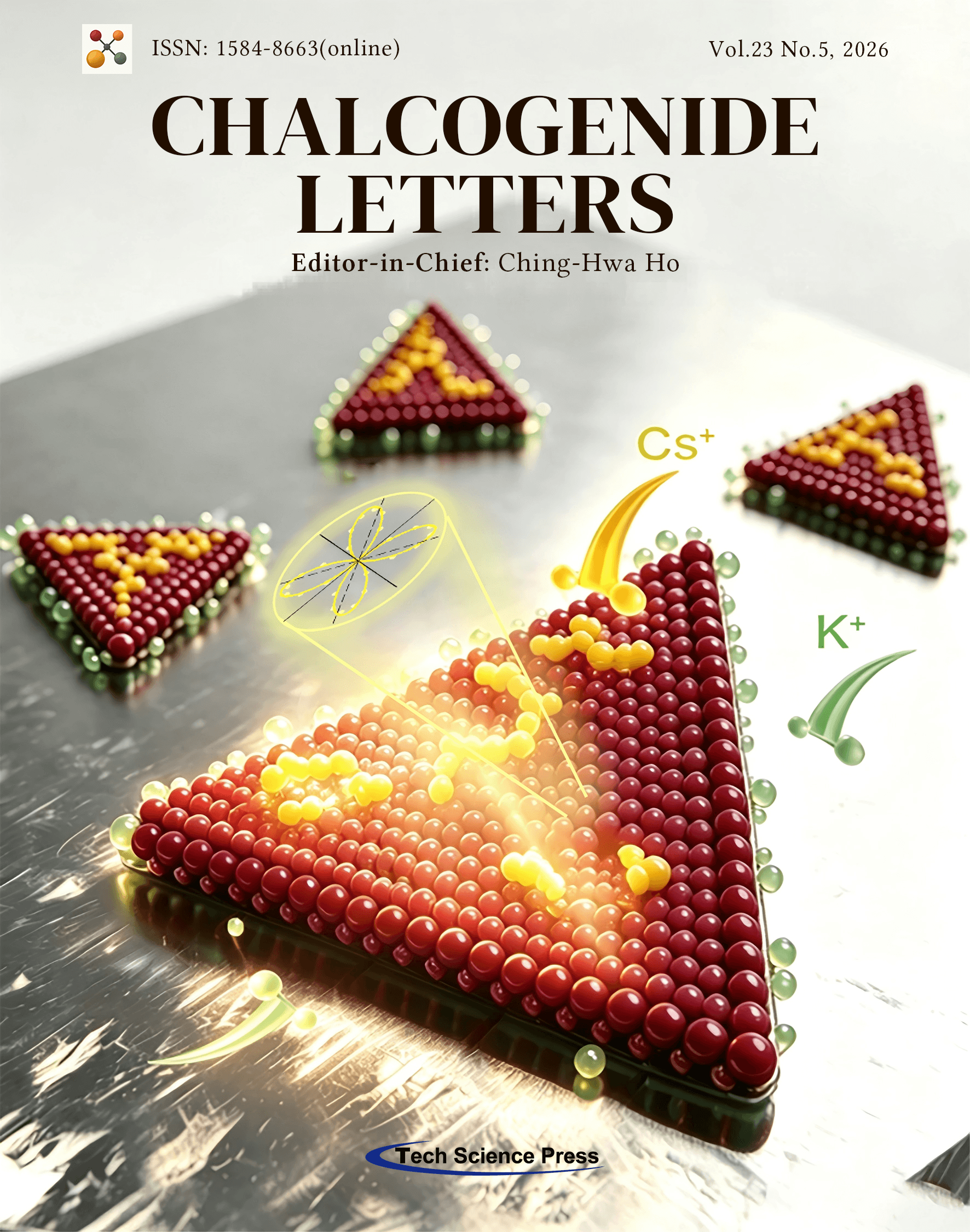
Home / Journals / CL / Vol.23, No.5, 2026
Special Issues
cover

On the Cover

The cover highlights the mixed salt-assisted growth of large-size ultrathin SnS₂ nanosheets, where the synergistic effect of CsCl and KI enables the formation of triangular single-crystalline nanosheets with lateral dimensions exceeding 200 μm and a thickness of only 1.8 nm. The central illustration depicts the ultrathin SnS₂ nanosheet grown on a mica substrate, while the enlarged atomic models emphasize its highly ordered crystal structure. The polarized Raman spectra and polar plots on the right demonstrate the substrate-dependent optical response, revealing the transition from intrinsic in-plane isotropy on SiO₂ to pronounced anisotropy on mica induced by interfacial lattice-mismatch stress. This work presents an effective strategy for morphology-controlled growth and anisotropy engineering in two-dimensional materials.
The cover image was created by Chatgpt and contains no copyrighted elements or misleading representations.

View this paper

  • Open AccessOpen Access

    ARTICLE

    Photoelectric Properties of Amorphous Selenium Thin Films Deposited by Thermal Evaporation

    Zhadyra Toreniyaz1, Guzal Ismailova1, Oleg Prikhodko1, Zhasulan Nakysbekov1, Tilek Kuanyshbekov2, Nurkadam Tolep1, Dmitry Terekhov3, Zhandos Tolepov1,*
    Chalcogenide Letters, Vol.23, No.5, 2026, DOI:10.32604/cl.2026.081101 - 02 June 2026
    Abstract Amorphous selenium (a-Se) thin films were deposited by vacuum thermal evaporation and investigated in planar photoconductive structures to evaluate their optical and photoelectrical properties in the low-field regime. SEM analysis showed continuous film coverage with a thickness of about 250 nm. Raman spectroscopy and X-ray diffraction confirmed the amorphous structure of the as-deposited films and the formation of trigonal crystalline selenium after annealing. Optical analysis based on transmission and reflectance spectra yielded an optical band gap E g = 1.96   eV and an Urbach energy E U = 0.083   eV ,… More >

  • Open AccessOpen Access

    ARTICLE

    First-Principles Insights into the Structural and Physical Properties of AgSbS2

    Tianjing Li1,*, Min Yao1, Wei Li1, Yue Yang1, Luping Qu1, Haijun Hou2, Hongli Guo3
    Chalcogenide Letters, Vol.23, No.5, 2026, DOI:10.32604/cl.2026.080386 - 02 June 2026
    Abstract This study focuses on monoclinic system AgSbS2, employing first-principles methods to calculate the structural, mechanical, optical, and thermodynamic properties. Specifically, geometry optimization yields a stable atomic structure with optimized lattice constants (a = 12.82 Å, b = 4.41 Å, and c = 13.19 Å). Furthermore, electronic structure analysis identifies AgSbS2 as a direct bandgap semiconductor with a bandgap of 1.456 eV, where the valence and conduction bands primarily originate from Ag-4d, S-3s, and Sb-5p states. Regarding the elastic properties, the calculated elastic constants, combined with Pugh’s B/G criterion, reveal excellent ductility. As for the optical properties, the static More >

  • Open AccessOpen Access

    ARTICLE

    Annealing-Induced Structural and Optical Modifications in SnS Thin Films and Their Impact on CO2 Gas Sensing Performance

    Seham Hassan Salman1, Sarmad Mahdi Ali1, Hawraa Hadi2,*, Dhufr Hadi3
    Chalcogenide Letters, Vol.23, No.5, 2026, DOI:10.32604/cl.2026.081302 - 02 June 2026
    Abstract Films of (SnS) with a thickness of 400 nm were deposited by the thermal evaporation technique to investigate the influence of annealing temperature on their Physics and CO2 gas-sensing characteristics. The deposited films were annealed at 200, 300, and 400°C. Structural characterization was performed using XRD, and the obtained results revealed that all samples possessed an orthorhombic crystal structure with a preferred orientation (301). The annealing treatment significantly improved the crystallinity of the films and reduced structural defects and lattice strain. Surface morphology investigations were performed using atomic force microscopy (AFM), which revealed noticeable modifications in… More >

  • Open AccessOpen Access

    ARTICLE

    Mixed Salt-Assisted Growth of Large-Size Ultrathin SnS2 Nanosheets and Their Anisotropy Study

    Yulong Lian1, Ruiqiang Wang1, Ziyan Ding1, Jinyang Liu1,2,3,*
    Chalcogenide Letters, Vol.23, No.5, 2026, DOI:10.32604/cl.2026.083268 - 02 June 2026
    Abstract The morphological regularity, thickness uniformity, and size controllability of two-dimensional materials play a crucial role in regulating their physicochemical properties. However, achieving a synergistic balance among these three factors remains a key challenge in the field. In this study, through a systematic investigation of 36 salt-assisted growth systems, we discovered that CsCl promotes the lateral growth of SnS2, while KI optimizes the crystal morphology. Using a CsCl/KI mixed salt system, we successfully grew triangular, ultrathin, large-area SnS2 nanosheets with a size exceeding 200 μm and a thickness of only 1.8 nm. Angle-resolved polarized Raman spectroscopy (ARPRS)… More >

  • Open AccessOpen Access

    ARTICLE

    Design and Optimization of a Novel Double-Heterojunction Lead-Free Cs2BiAgI6 Perovskite Solar Cell with PCBM/C60 Bilayer ETL and CdTe HTL: Numerical Investigation

    S. D. Al-Sahafi*
    Chalcogenide Letters, Vol.23, No.5, 2026, DOI:10.32604/cl.2026.082364 - 02 June 2026
    (This article belongs to the Special Issue: Chalcogenide Thin Films and Solar Cells for Optoelectronic Applications)
    Abstract In this study, a lead-free double perovskite solar cell structure based on Cs2BiAgI6 was simulated and optimized to enhance photovoltaic performance. The device architecture follows the configuration: ITO/PCBM/C60/Cs2BiAgI6/CdTe/Au. The thicknesses of the electron transport layer (ETL), absorber layer, and hole transport layer (HTL) are systematically optimized to evaluate their impact on key performance parameters. The results indicate that optimal performance is achieved with 600 nm thicknesses for all ETLs and HTL, and 2 μm for the Cs2BiAgl6 absorber. Under these conditions, the device exhibits a short-circuit current density of 23.23 mA/cm2, an open-circuit voltage of 1.08 V, More >

  • Open AccessOpen Access

    ARTICLE

    Zn Vacancy-Regulated Zn0.4Cd0.6S for Enhanced Charge Separation and Boosted Photocatalytic H2O2 Generation

    Yuanyi Zhang, Yang Gu, Yuxin Lan, Zhenyu Wang, Wei Yan, Yingcong Wei, Jing Xu*
    Chalcogenide Letters, Vol.23, No.5, 2026, DOI:10.32604/cl.2026.082986 - 02 June 2026
    (This article belongs to the Special Issue: Chalcogenide Materials for Sustainable Environment)
    Abstract Photocatalytic H2O2 synthesis from O2 is a green and environmentally friendly route. However, due to the limitations of quick recombination of photogenerated electrons and limited O2 activation ability, photocatalytic reactions often exhibit low efficiency. In this study, Zn vacancy-engineered Zn0.4Cd0.6S (ZnV-ZCS) photocatalysts were successfully constructed via a hydrothermal strategy using L-cysteine as a coordination agent. The optimized ZnV-ZCS-10 catalyst achieves an impressive H2O2 production rate of 44.39 mmol/g within 1 h under 425 nm irradiation, approximately 2.3 times higher than that of pristine Zn0.4Cd0.6S (ZCS). Structural characterization and cycling performance tests confirm that the introduction of Zn vacancies does More >

    Graphic Abstract

    Zn Vacancy-Regulated Zn<sub>0.4</sub>Cd<sub>0.6</sub>S for Enhanced Charge Separation and Boosted Photocatalytic H<sub>2</sub>O<sub>2</sub> Generation

Per Page:

Share Link